TSMC prepares to challenge Samsung’s lead in Panel-Level Packaging for AI chips
Chip foundry giant TSMC is reportedly building out a full supply chain for Panel-Level Packaging, the next-generation semiconductor packaging technology where Samsung Electronics has held a quiet, durable lead for years.
ETNews, via SemiconductorsX, reports that TSMC is in talks with equipment and materials suppliers to lock in a mass production system based on Panel-Level-Packaging technology, and the target is early next year.
After absorbing the PLP business from Samsung Electro-Mechanics in 2019, Samsung spent years quietly applying the technology to mobile application processors and power management chips.
TSMC didn’t need PLP when conventional wafer-level packaging was keeping customers happy. Meanwhile, the demand for bigger chips at higher volumes changed the prospect overnight.
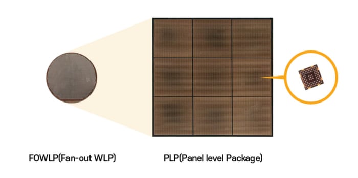
What is Panel-Level Packaging
Conventional packaging happens on round wafers.
A 300mm wafer wastes the edges, all that curved geometry that can’t fit a complete chip.
PLP moves the process to a rectangular panel, roughly 600x600mm, offering five to six times the output from the same process.
Notably, TSMC stood up a pilot line in 2025, evaluated it, and is now moving toward large-scale production. The company has reportedly already secured customers among global AI chip players.
Samsung isn’t standing still either. It’s pushing PLP into high-performance computing and AI semiconductors, and it’s eyeing glass substrates as the next packaging frontier.
The post TSMC prepares to challenge Samsung’s lead in Panel-Level Packaging for AI chips appeared first on Sammy Fans.