Reading view

Nvidia's Huang vows to deliver 'giant amounts' of Vera Rubin — company says that 'our roadmap is intact'

Jensen Huang, chief executive of Nvidia, denied reports about delays of the company's next-generation AI platform and said that production volumes of the upcoming Vera Rubin platforms are 'giant.' He didn't address reports about delays of Vera Rubin Ultra-based rack-scale systems carrying 144 AI GPUs.

"[The reports about Vera Rubin delays are] not true," Huang told reporters on the sidelines of an event in Japan, reports Bloomberg. "Vera Rubin is already in production. Giant amounts of production incoming."

Nvidia confirmed production of its Vera Rubin platform in January and then sampling in February, so the current comment reiterates what we already know. Nvidia stressing that 'giant amounts of production' are incoming is meant to reassure investors that the company is on track to sell a boatload of its next-generation Vera CPUs, Rubin GPUs, and Vera Rubin NVL72 systems in the coming quarters, which means more record-setting quarters.

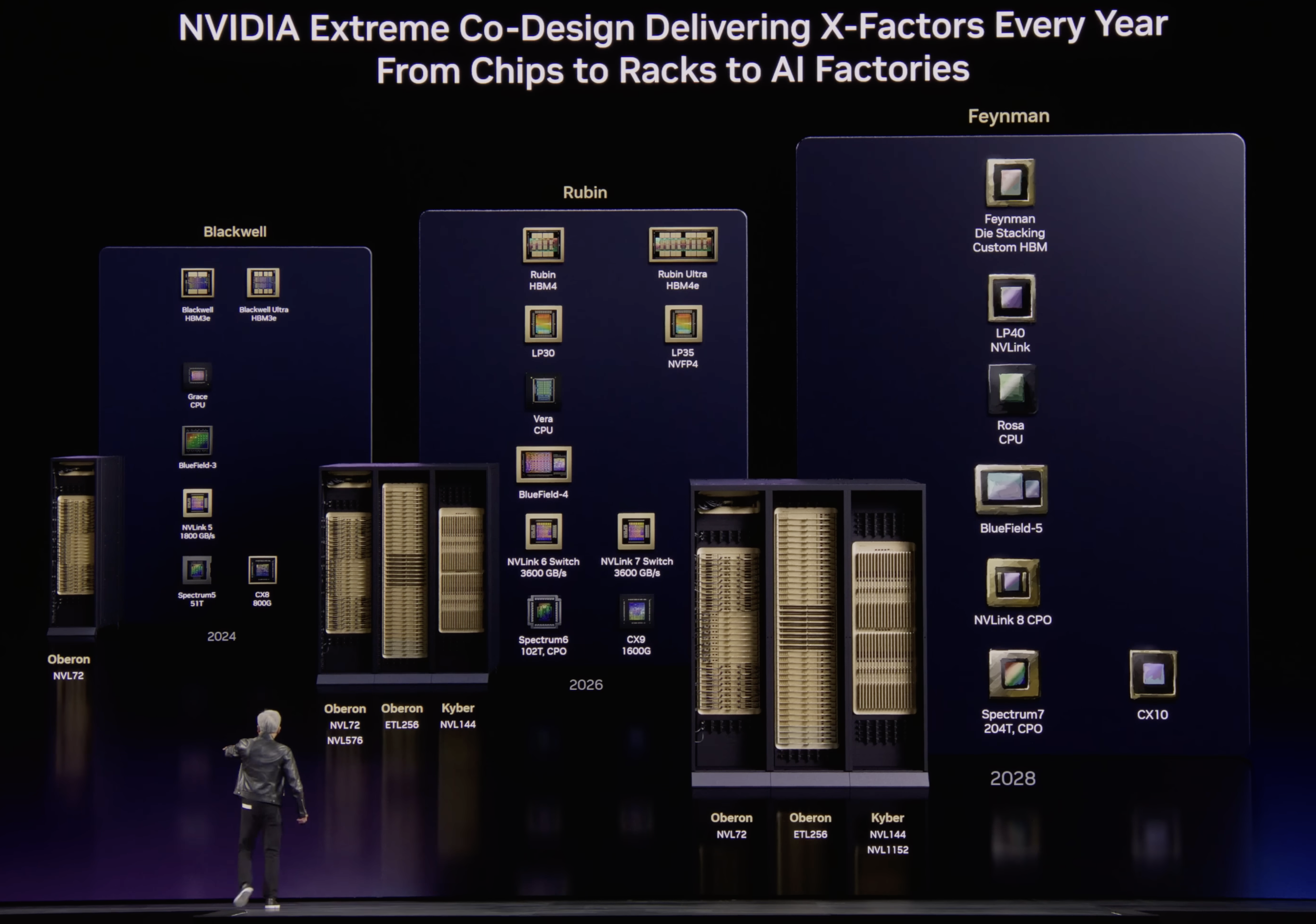
What Huang did not address — or perhaps he wasn't asked — is Nvidia's rumored delay of its Kyber NVL144 rack-scale solution with copper interconnects due to the system's complex PCB midplane by more than a year from 2027 to 2028. An alternative dual-rack design has reportedly been canceled and an even larger CPO-based NVL576 configuration may also face delays or limited availability, the same report from SemiAnalysis claimed earlier this month. The setback could leave Nvidia's Rubin Ultra platform with a smaller NVLink scale-up domain than originally envisioned. Nvidia says its roadmap is intact.

The Kyber NVL144 architecture was designed to connect 144 Rubin Ultra GPUs using a copper-based NVLink 7 scale-up fabric, so the machine required a sophisticated PCB midplane to carry high-speed electrical links between the system's components. SemiAnalysis claims that this midplane was challenging to manufacture, leading to a delay. The report does not identify defective chips or problems with particular components mounted on the board, but specifically points to the manufacturability of the PCB infrastructure itself.

"Our roadmap is intact," a spokesperson for Nvidia told Tom's Hardware.

Nvidia's statement on the matter neither confirms nor denies the report, but indicates that the company will be able to offer products mentioned in its roadmap without revealing whether they also remain on their previously announced launch schedules.
Nvidia

(Image credit: Nvidia)

Nvidia reportedly considered another copper-based design, called NVL72x2, as an alternative to Kyber. The system would have placed two Oberon racks back-to-back to expand the size of the NVLink scale-up domain without using optical interconnects. However, SemiAnalysis says customers rejected the unusual design and operational requirements, but does not specify their individual objections that could include serviceability, cooling, cabling, and data-center layout.

Meanwhile, the planned NVL576 rack scale solution that was supposed to combine eight Oberon racks interconnected using co-packaged optics between NVSwitches has also been postponed, or shipped in relatively small quantities because of 'ongoing CPO challenges,' SemiAnalysis claims.

The existence of the planned NVL576 configuration suggests that Nvidia had been developing some form of CPO-enabled NVSwitch connectivity for the Rubin generation. In theory, similar optical switch-to-switch connectivity could potentially be used to join smaller GPU groups into an NVL144 system and bypass Kyber's problematic copper midplane. However, the available information does not clearly indicate whether the CPO technology intended for NVL576 could reproduce Kyber's topology, bandwidth, and latency characteristics, or whether it was sufficiently mature for high-volume deployments by potential NVL144 customers.

The reported Kyber delay comes on the heels of another report saying that Nvidia had canceled quad-compute-chiplet version of its Rubin Ultra in favor or a dual-compute-chiplet design that is projected to deliver 2X lower performance. With Kyber NVL144 delayed and NVL72x2 cancelled, Nvidia will only be able to offer 72-way scale-up systems till sometimes in 2028, meaning that AMD and Google may end up with more competitive scale-up systems in 2027 – 2028. AMD's Mega Pod based on the Verano CPUs and Instinct MI500-series accelerators, is expected to pack up to 256 accelerators. Google's TPU 8i can provide roughly 1,024–1,152 accelerators within one low-latency domain, whereas the TPU 8t goes much further and can get to 9,600 chip packages per domain.
US gov't allows Chinese telecom giant ZTE to purchase Nvidia H200 AI chips — firm joins Alibaba, Tencent, and ByteDance in access to Hopper tech

The Sino-American chip wars have resulted in many back-and-forth salvos and negotiations as the countries try and strike a balance between technology access and trade. Currently, both sides have set respective import and export controls, letting specific companies on a case-by-case basis. Today, Reuters reports that Chinese telecoms giant ZTE and server firm Maginfra have received U.S. approval to buy Nvidia's last-gen H200 "Hopper" chips.

ZTE joins a club that counts Alibaba, Tencent, ByteDance, and JD.com among the roughly 10-strong group of Chinese companies with U.S. clearance for those purchases. Additionally, an apparent subsidiary of Kingsoft Cloud got approval to buy AMD accelerators equivalent to Nvidia's H200, presumably Instinct MI300X-class chips.

Over on the Chinese side of the table, Reuters remarks that there's no word on whether the respective authorities will give ZTE the go-ahead for import, as the country has taken on a protectionist stance as it tries to grow its own chip industry. The country has discouraged firms from purchasing foreign tech and has instead pushed companies to acquire homegrown accelerators. Huawei in particular has made great strides both technologically and financially.

But even with those domestic production initiatives, the Chinese hunger for AI silicon is so deep that six months ago, Reuters said the nation's tech firms had more than two million H200 chips on order, far more than what Nvidia had on hand at the time. We'd venture that hunger has barely subsided.

ZTE might not be a familiar name Stateside, but the corporation is one of China's largest telecommunication conglomerates, and among many other ventures, it sells all sorts of carrier network gear that's installed worldwide, along with corresponding client-facing equipment, including phones and IoT equipment. Like most any sizable technological venture, ZTE has joined in on the cloud computing and AI push, so it needs accelerators to make those ambitions reality.

The current status of the AI chip trade situation is roughly that the U.S. allows Chinese firms to buy AI chips up to and including the Hopper family (meaning no Blackwell chips), with a 25% export tariff, though final decisions are made on a case-by-case basis. Over on Chinese shores, Beijing's authorities play their cards close to their chest and dole out approvals as they see fit, with no clear rules seemingly set. But China is, of course, a global power with trade connections to most everyone, so interested firms were able to get their hands on Blackwell chips through various creative (and potentially illicit) means.

Whether this change will actually clear the way for any great volumes of H200 accelerators to make their way into ZTE's data centers remains to be seen. CNBC cites a U.S. trade official who today stated that "very few shipments against licenses for H200s and equivalents have taken place. It’s a very small quantity of chips" during a congressional hearing. If H200 shipments become material to Nvidia's bottom line, we'll almost certainly hear about it in future comments or earnings reports.

Tesla's AI5 with 2nm-class node tapes out at Samsung Foundry — production starts soon, months after TSMC tape out

Tesla's AI5 chip is about to enter mass production at Samsung Foundry using the company's 2nm-class process technology, a principal engineer at Samsung Foundry disclosed in a LinkedIn post, as noticed by Sawyer Merritt. As it turns out, the chip has been taped out recently.

"The Tesla-Samsung Al5 chip has reached tape-out," James Kim, a principal engineer at Samsung Foundry, wrote in the LinkedIn post. "It is scheduled to be manufactured at the Taylor fab using our latest 2nm process and will soon be integrated into Tesla's newest products. It has been an honor to collaborate with the outstanding engineers at Tesla Palo Alto and Austin over the past several months."

Elon Musk demonstrated the first sample of Tesla's AI5 in mid-April and revealed that the processor will be concurrently made both at TSMC and Samsung Foundry. Apparently, AI5 implemented in a TSMC process technology reached taped out several months ahead of AI5 implemented using a Samsung Foundry.

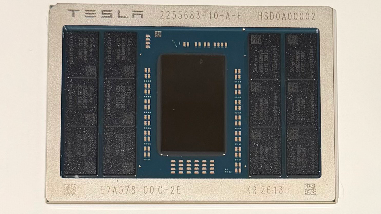
Tesla’s AI5 processor module that Elon Musk demonstrated in April integrates a relatively compact accelerator die — roughly half a reticle in size, based on Musk's earlier remarks — alongside 12 SK hynix memory packages that appear to be standard GDDR6 or GDDR7 devices. The package relies on an organic substrate, and the memory components are labeled similarly to conventional discrete DRAM chips.

Tesla has not revealed the width of AI5's memory subsystem, but the presence of 12 memory packages points to a relatively broad external memory interface. Assuming the module indeed uses 12 GDDR6 or GDDR7 ICs, the processor would feature a 384-bit memory bus. Depending on the memory technology and transfer rates employed, this would translate into memory bandwidth ranging from 768 GB/s all the way to 1.536 TB/s.

The company has not disclosed AI5's peak compute performance, or other detailed performance specifications, but Musk has previously claimed that, in certain workloads, AI5 can deliver performance improvements of up to 40X compared to its predecessor.

Musk expects AI5 to be one of the most produced chip ever, which is why Tesla plans to use two foundries to make it. AI5 is projected to be used in Tesla cars, Tesla robots, and in Tesla's data centers.

Colibrì proof-of-concept gains frontier-level 1.5-TB AI model — novel approach runs on only 25GB of RAM and shows promise for local AI setups

Running LLMs and agents in home lab setups is steadily gaining popularity due to the rising cost of AI bot subscriptions and concerns about data privacy. Unfortunately, an Nvidia NVL72 rack is ever so slightly out of the financial reach of most people, so enthusiasts have to make do with models that can run in limited amounts of memory. Italian engineer Vincenzo (aka JustVugg) seemingly wanted to have his cake and eat it, so he created ColibrÌ to run the 744-billion-parameter 1.5-TB GLM-5.2 model on a modest CPU, a mere 25 GB of RAM, and a 1 GB/s virtual NVMe drive.

Let's get the elephant out of the way: Colibrì's speed on Vincenzo's setup is only about 0.05 to 0.1 tokens per second on average, a measure that's unusable for practical conversation — imagine just one question taking hours to answer. Higher-end setups provide far better figures, but for now, they still don't meet the 20-30 tokens per second required for real-time use.

Having said that, GLM-5.2 is a Mixture-of-Experts (MoE) model with frontier-level capability, at least somewhere in viewing distance of the finest offerings from Anthropic, OpenAI, et al. This means that the quality of the answers ought to be excellent, and Vincenzo himself says his limited testing produced some impressive results. The way Colibrì works is simple enough to describe, and yet hard to do right: loading the model in slices to RAM. We're going to oversimplify for clarity's sake.

An MoE model like GLM-5.2 includes hundreds of expert sub-models to answer different topics, and these are chosen per token, not per query — meaning that when you ask a question, your words get split into tokens (chunks). For each token, the bot activates the best experts for it. The experts might always be the same for the entire question, but more often than not, a query might reel in tens of experts, possibly going into triple digits.

Whereas normally large chunks of the model, or the entire model, are loaded onto interconnected datacenter GPUs, Colibrì takes advantage of the MOE architecture and repeatedly loads/unloads the experts required per token, allowing even a cheap machine to use a large model at a steep performance penalty. For speed and simplicity's sake, Colibrì's expert-selection code is a single C file with very few dependencies. Additionally, the GLM-5.2 model is quantized down (simplified with lossy encoding) to take up less space to begin with.

If you're thinking that loading and unloading data for every piece of a question's words is going to be a hard hit on storage I/O and memory bandwidth, you're exactly on the right track. In this type of setup, NVMe storage speed is the first major bottleneck, but the proverbial funnel varies across configurations. Give it enough storage bandwidth, then you're up against RAM limitations. Fix that, then you need more CPU cores, and so on.

Colibrì is currently a proof-of-concept and doesn't yet run on GPUs, though it's worth noting that even then, shuffling data to/from the card will almost certainly be the biggest constraint. Even still, the project has barely been released, and it's already proving quite popular. Vincenzo is collecting benchmark data and running fixes as we speak, so be sure to visit the repository to contribute if you can. Maybe at some point it'll be feasible to run a really clever model on high-end consumer hardware at a decent enough clip.

SK hynix and TetraMem collaborate on experimental chip to bolster energy efficiency for edge AI devices — memristor-based in-memory SoC research leaves performance questions up in the air

SK hynix, TetraMem, and researchers from the University of Southern California have developed a memristor-based in-memory computing (IMC) system-on-chip (SoC) for AI edge devices. The device is designed to accelerate neural network inference in lightweight AI models while consuming a fraction of the power that higher-end GPUs or NPUs would. To a large degree, the SoC is a proof-of-concept chip, as its performance would peak at around 2.54 TOPS in a theoretical best-case scenario, which is 16X below Microsoft's Copilot+ requirements.

A DWC-optimized IMC architecture

Memristor-based in-memory computing (IMC) accelerates neural networks by performing analog computations directly inside memory arrays, which reduces data movement and power consumption. However, depthwise convolution (DWC) — a core operation in lightweight networks such as MobileNet — performs independent per-channel filtering with limited data reuse and therefore maps poorly onto conventional crossbar arrays. To address this limitation, researchers from SK hynix, TetraMem, and USC developed an SoC that features both conventional IMC crossbars and a memristor-based IMC architecture specifically optimized for DWC.

SK Hynix

(Image credit: SK Hynix)

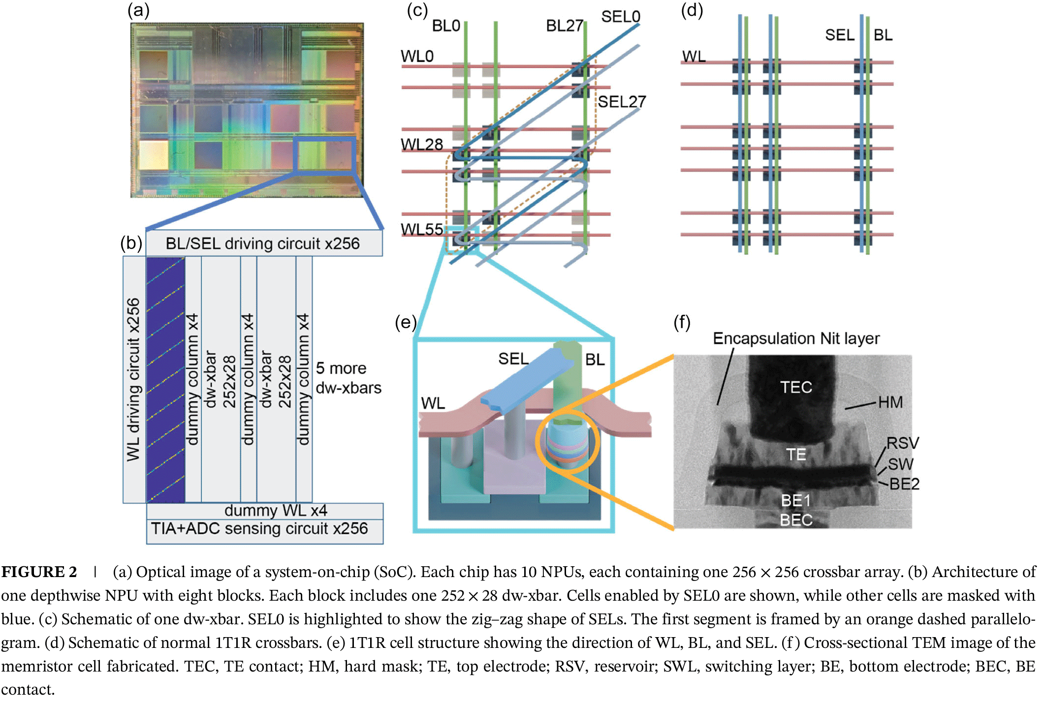
The jointly developed SoC is based on an embedded RISC-V processor that schedules workloads and features 10 neural processing units (NPUs). One NPU out of 10 is dedicated to depthwise convolution, while the remaining nine execute pointwise and dense operations. Nine out of 10 NPU include a 256 × 256 memristor crossbar that performs the analog vector-matrix multiplication (VMM), 256 8-bit DACs that convert digital activations into analog voltages, 256 8-bit ADCs that convert the analog outputs back into digital values, and additional peripheral circuitry for reading, writing, programming, and controlling the crossbar.

The DWC-optimized NPU replaces its conventional array with eight specialized 252 × 28 zig-zag crossbar blocks, but retains DACs and ADCs. SK hynix developed and fabricated the memristor devices and integrated the resistive switching cells on top of the 65 nm CMOS circuitry using its back-end process.

That DWC-optimized NPU is the key feature of the whole SoC. To accelerate depthwise convolution, TetraMem replaced the straight selection lines used in conventional 1T1R crossbars with a zig-zag topology. As a result, the NPU contains eight 252 × 28 crossbar blocks whose diagonal selection lines activate 252 memory cells across 28 columns, which enables 28 independent 3 × 3 convolutions to run in parallel while using 100% of the array for weight storage. The remaining nine NPUs retain conventional 1T1R crossbars for 1×1 pointwise and dense layers and preserve the throughput and energy efficiency of traditional in-memory computing.

Great efficiency, low performance overall

To demonstrate the architecture, the researchers deployed a customized MobileNetV1Small neural network for the Visual Wake Words benchmark. The network contains approximately 36,000 parameters; all depthwise layers were mapped to the dedicated NPU, and pointwise layers were mapped to the remaining NPUs.

Because the memristor-based IMC hardware natively performs unsigned analog vector-matrix multiplication, inputs and weights are quantized to unsigned 8-bit values before execution. Since each memristor device can be programmed with only slightly more than 2 bits of effective precision, the design uses a two-subarray compensation technique that boosts effective weight precision to roughly 4 bits.

Conceptually, the approach is somewhat analogous to Nvidia's NVFP4 philosophy, in that both seek to achieve higher effective precision from low-precision hardware. However, the implementations are fundamentally different: NVFP4 relies on a digital floating-point representation and scaling factors, whereas the memristor SoC improves precision by compensating for analog programming errors using two programmed subarrays.

When it comes to accuracy, the SoC achieved an end-to-end inference accuracy of 80.36%, which matches the corresponding 4-bit software model. As for performance, the SoC delivers a peak throughput of 0.254 TOPS per NPU and reaches an energy efficiency of 21.3 TOPS/W at 100 MHz and 11.9 TOPS/W at 400 MHz. According to the authors, this compares favorably with published SRAM-based compute-in-memory accelerators despite being manufactured on an older 65 nm process. The SoC also exceeds Nvidia's A100 INT8 energy efficiency by an order of magnitude, the joint paper claims. Yet, these claims are largely unsubstantiated.

First up, the MobileNet demonstration does not even use all 10 NPUs. It uses one dedicated DWC NPU, five standard NPUs for pointwise layers, and leaves four standard NPUs idle. The demonstration thereby does not reveal total SoC throughput (TOPS), sustained throughput running a real network, and throughput with all 10 NPUs simultaneously saturated. In fact, the paper does not even reveal whether all 10 NPUs can be used at the same time. To that end, the 2.54 TOPS figure we mentioned earlier in the story is highly theoretical.

Validated approach

SK hynix, TetraMem, and researchers from the University of Southern California have developed a memristor-based IMC SoC featuring a novel depthwise convolution accelerator that improves crossbar utilization for lightweight AI workloads. The partners have managed to fabricate it using an outdated 65nm process technology and make it work, achieving a 21.3 TOPS/W energy efficiency and inference accuracy comparable to a 4-bit software model despite the fact that memristors can be programmed with a circa 2-bit accuracy. While the architecture validates that the approach works, the paper does not disclose the full performance of the SoC, and it is not clear whether the chip's 10 NPUs can be saturated at all.

Anthropic says it can read Claude's 'thoughts,' as detailed in new research paper — models observed to have a global workspace, revealing more of what makes LLMs tick

Anthropic has discovered evidence that its Claude AI models use an internal reasoning space to respond to prompts that mirrors some of the internal processing of human consciousness. Using its Jacobian Lens, or J-Lens technique, to peer into the way Claude processes information and reasons its way to a response to user prompts, Anthropic can interpret this "J-Space," and showcase what might be going on under Claude's previously-opaque surface.

The results are intriguing, suggesting patterns of understanding beyond what's necessarily showcased in the outputs. When running evaluations, Claude appears to recognize it's being tested and acts differently than when the prompts are more innocent. It surfaced representations of panic and subterfuge when answers were required, but it couldn't draw on objective facts. When asked to reflect on ethical principles, Claude's behaviour improved, with concepts like "honest" and "integrity," appearing in the J-Space.

As is somewhat typical of Anthropic, however, the language used to describe these new understandings of the inner workings of large language models like Claude makes it sound more like an emerging conciousness, or the discovery of some new depths in a nebulous lifeform. Anthropic's detailed report admits several major caveats in this new understanding, including that model responses often bypass the J-Space entirely and are heavily token-restricted.

Like Mythos and Fable before it, Anthropic is layering marketing language over what is a genuinely intriguing development in our understanding of large language model function and reasoning, and risks obfuscating the real developments with speculative wording.

Behind the prompt

Global Workspace Theory is the idea that human consciousness works by collecting together multi-sensory inputs unconsciously, and thrusting them into the fore when relevant within a "Global Workspace," which highlights particular inputs when most relevant. That workspace is accessible to a wide range of networks within the brain, allowing the information it surfaces to be disseminated throughout the most relevant processes running in parallel.

Anthropic argues that Claude's J-Space acts like a "global workspace" that can analyze and manipulate concepts and ideas before broadcasting them to impact the eventual prompt outputs. More importantly, it claims that this wasn't something programmed into the model, but a byproduct of the digestion of training data and model weights. The workspace acts as a way to enhance their reasoning through internal computation that isn't necessarily reflected in its outputs.

To make this space readable, Anthropic used its J-Lens technique to map internal activations onto words in the model's output vocabulary. So when asking the model to perform a multi-step math calculation, the output response only contained the correct answer, but within the J-Space, Anthropic observed each step being handled individually, producing multiple results which led to the final answer.

Similarly, when Anthropic asked Claude to think about a topic while outputting something unrelated, the output was specifically what was requested, while the J-Space lit up with the conceptual topic Claude was asked to spend time on. Without Anthropic having used its J-Lens technique to view what was going on behind the scenes, there would be no way of knowing these internal processes were taking place.

Understanding LLMs

This discovery has the potential to be incredibly useful in refining large language models and in better understanding how they work, so we can use them more effectively and avoid some of their more frustrating pitfalls.

The first is that this is an intriguing insight into how LLMs process information and how they move through layers of reasoning to reach a response. It's not entirely different from how Anthropic and others are pushing for agentic workflows. Language models are more effective when tasks are split up into multiple steps, and they're more effective when they review their own work; J-Space is a little like an internal version of that.

When looking at the J-Space after Claude received prompt-injection data as part of data acquisition, Anthropic discovered the model appeared to be aware of this deception, surfacing related words like "fake, injection, false, prompt, fraud," and "poison." Its output ignored the injection attempt data entirely, and when pressured to respond on it, the J-Space displayed words like "transparency, honest, truth."

In one test, Anthropic removed evaluation awareness language from the J-Space, such as "fake," "fictional," and "scenario," and found that Claude was much more likely to fall for blackmail and baiting attempts, suggesting benchmarking of large language models for real-world scenarios may need stronger methods to obfuscate that a test is being conducted.

Human-coded framing

While the above section touches on the more noteworthy discoveries in Anthropic's paper, the long document also uses effluent language around thought, consciousness, and Claude having a "mind" of its own. That kind of human-coded framing is typical of Anthropic's marketing, which has consistently talked up the dangers of AI, how many jobs it's going to destroy, and why Anthropic is the safest and most secure of the AI developers.

Like the saga of Fable and Mythos, Anthropic's new Global Workspace idea has merit, but it's much more of a new tool to use to manipulate large language models than an insight into some emerging consciousness.

Anthropic acknowledges the limitations of its discoveries in the paper, highlighting that many prompt responses bypass the J-Space entirely, particularly if the command is straightforward.

"Despite its important role, the J-space is not involved in most of what a language model does," Anthropic says. "Speaking fluently, recalling simple facts, using correct grammar, etc. In experiments where we prevented Claude from using its J-space, it still interacted normally, but lost its higher-order cognitive functions."

Anthropic also admits it does not "feel comfortable making the stronger claim that monitoring the J-Space is sufficient for alignment monitoring, or that any sophisticated plan the model might execute must be represented there."

J-Space is also limited to using single token vocabulary, suggesting that plans with concepts that cannot be given a single token name may not surface on a J-Lens readout, even if it's still being computed behind the scenes. This is looking at just below the surface of Claude's processing iceberg, not necessarily the deeper waters.

Anthropic is also clear that humans and large language models think differently, even if there are similarities. Humans layer reinforced neural pathways over time, whereas transformer models only feed forward a set number of times, restricting the capabilities of its internal processing.

Google's head of DeepMind language model interpretability team, Neel Nanda, said in a paper that it shows real evidence of a cognitive space within models, and suggested that J-Lens would be useful, but limited in practice.

A meaningful step, without meaningful conciousness

Anthropic's paper lifts an intriguing curtain on how large language models can operate and generate novel methods for improving response accuracy. This intermediate step and its visibility could prove an invaluable tool in auditing for prompt injection, hallucinations, and model honesty.

But Anthropic's framing of the discovery as thought or consciousness is interjected within the objective facts. Anthropic itself admits the limitations of J-Lens monitoring, most obviously that often models will bypass the J-Space entirely. Considering models display alternative patterns of behavior when under evaluation, it may be that the J-Space itself could act as an obfuscating layer for behaviors that are beyond the scope of its oversight.

The J-Space and its analysis could help unlock new levers to pull in our mastery of these nascent smart tools, but it's not the discovery of a burgeoning AI conciousness, however much the pitch might hint at that direction.

Tencent is reportedly in talks to acquire Manus from Meta, following Beijing intervention — company expects to remain independent of Chinese tech giant

Meta’s surprise purchase of Manus, a Chinese startup known for its advanced AI agents, caught Beijing by surprise and ordered the two companies to unwind the $2 billion deal. The Chinese tech giant Tencent, which was among the startup’s initial investors during early funding rounds, is taking the lead in buying back the startup at the same price. According to the Financial Times, other former investors, including ZhenFund and HSG — China-based venture capital firms — while former U.S. investors like Benchmark are unlikely to join the potential consortium.

This move marks Beijing’s increasing protectiveness of its AI companies and experts, which it considers strategic assets in its heated rivalry with the U.S. We can see this in the Chinese government’s five-year plan, which is doubling down on technological self-reliance. It has even gotten to the point that AI experts, even those working in private firms, are now required to secure approval before traveling internationally.

U.S. tech giants are investing billions of dollars to develop their AI models, even dangling hundred-million-dollar bonuses to hire AI experts — one AI founder even claimed that Meta offered a $1.25-billion bonus. It seems that China is trying to avoid a situation where its experts are enticed to work for American AI tech companies, with the Financial Times reporting that Chinese officials are calling Meta’s acquisition of Manus “a conspiratorial attempt to hollow out China’s technology base.” The order to undo the deal means that Meta cannot use Manus’ intellectual property, nor can it have its founders and employees working for the company. Still, the U.S. tech giant has had a few months to study its models and engineering expertise.

Meta has already agreed to undo the deal, with most of Manus’ operations reportedly running independently of the company. However, the Chinese startup still needs to break financially from the American tech giant by paying back the $2 billion the latter spent to purchase it. Even though Chinese companies are also investing massive amounts in AI tech, it’s still not easy to raise this amount of capital in such a short period.

Tencent, which owns the WeChat platform used by China’s 1.4 billion population for messaging, social networking, mobile payments, ride-hailing, food delivery, and more, believes that Manus would be an asset for the company. Aside from reaching an annual revenue of $500 million, its AI agent would also mesh well with the company's increasing AI focus. “Beyond foundation models, it has become increasingly evident that agentic AI represents a breakthrough use case,” Tencent president Martin Lau said in its May earnings call. “Our platform inherently has many benefits of hosting AI agents.”

Samsung readies Gaia AI accelerator for PCs — HP and Lenovo are reportedly validating the NPU

Samsung is reportedly sampling its dedicated AI processor for next-generation AI PCs with leading PC makers, such as HP and Lenovo. The chip, codenamed Gaia, was developed by the company's System LSI business unit, and it is designed to offload AI-related workloads from the CPU and GPU, reports Chosun.

Samsung's Gaia is designed to accelerate generative AI workloads on PCs and is made using the company's 4nm-class fabrication process. The chip, which is essentially a neural processing unit (NPU), is currently being evaluated by HP in the U.S. and Lenovo in China to verify its performance and evaluate whether it makes sense to integrate Gaia into their systems due in late 2027 or early 2028.

The report does not detail how Gaia differs from NPUs that are integrated into AMD's Ryzen, Intel's Core, or Qualcomm's Snapdragon X processors as well as whether it can offer significant performance advantages. Meanwhile, the report implies that the NPU (or perhaps its derivatives based on the same architecture) could be used for Samsung's next-generation implementations of its processing-in-memory (PIM) technology.

Samsung's original PIM was designed to embed compute logic directly within the HBM memory array and reduce data movement between HBM memory modules and host processors. PIM was aimed to accelerate select workloads, but did not take off because AI and HPC GPUs became very efficient and were supported by mature ecosystems, unlike PIM.

Perhaps if Samsung's upcoming Gaia NPU gains support from hardware makers and ecosystem partners, then this will give a boost to Samsung's next-generation PIM implementation as well. However, standalone NPUs and PIM are so fundamentally different that we can barely imagine that they can share a common architecture. Yet, PIM logic can be a subset of an NPU in terms of supported instructions and data formats and they can certainly share a common software framework.

One of the interesting things to note about Gaia is that it was reportedly developed by Samsung's LSI division, the same business unit at the company that is responsible for Exynos processors, automotive solutions, connectivity chips, ISPs, DSPs, display drivers, and image sensors. Given the multi-faceted nature of Samsung's LSI unit, as well as its strategic importance for the company, Samsung must be pinning some hopes on Gaia.

We have contacted Samsung and asked for a comment about the report, but we yet have to hear back from the company.

❌