Tech War Intensifies: China’s Lithography Breakthrough Challenges U.S. Semiconductor Edge

Key Highlights:
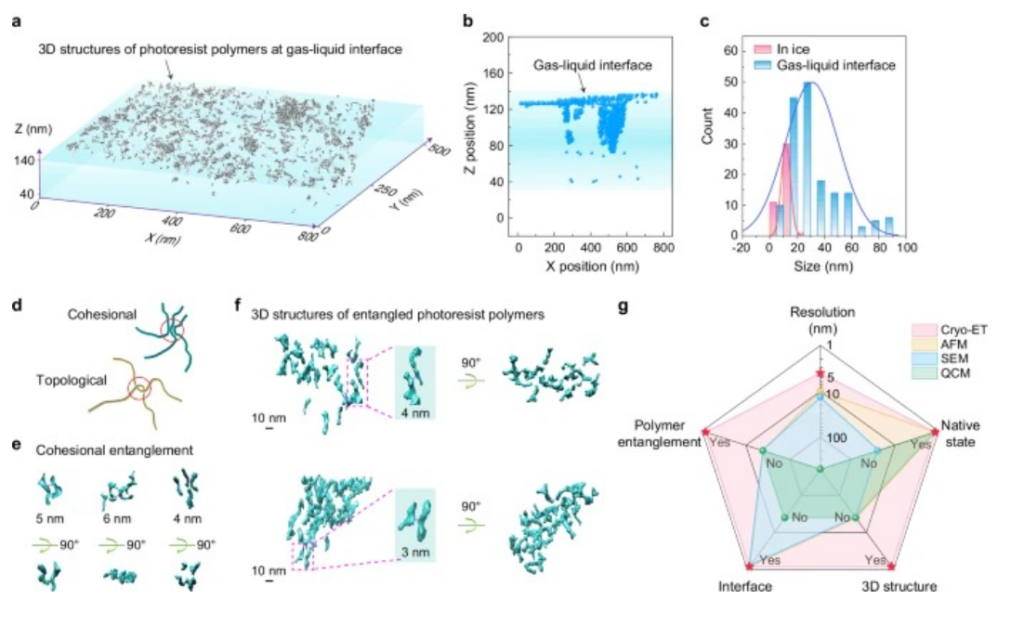
- Chinese researchers at Peking University achieve a world-first visualization of photoresist behavior using cryo-electron tomography (cryo-ET).
- The discovery could help China reduce reliance on foreign photoresist materials and improve chip yields at advanced nodes.
- The breakthrough deepens the ongoing U.S.-China tech rivalry, potentially influencing global chip prices and supply for everyday electronics.
China’s Breakthrough in Lithography Materials
China has achieved a significant milestone in semiconductor technology that could alter the global landscape in chip manufacturing. A team led by Professor Hailin Peng from Peking University, working with domestic collaborators, has developed a method to reduce defects in chip lithography dramatically. Using cryo-electron tomography, a technique more commonly seen in biology, the researchers visualized how light-sensitive photoresist materials behave at the molecular level during chip production.
For the first time, scientists were able to see how photoresist polymers interact in liquid film and at gas–liquid interfaces, uncovering the hidden causes of defects that limit chip yields. The team’s new process reportedly eliminated up to 99% of these defects under industrial conditions, marking a turning point for China’s semiconductor ambitions.
Why This Matters
Photoresist materials are essential for defining nanoscale circuits on silicon wafers. Until now, China has depended heavily on imports, with over 90% of its photoresist supply coming from Japan. By developing its own high-performance photoresist and imaging technology, China is moving closer to self-reliance in one of the most critical areas of chipmaking.
The discovery could improve manufacturing yields in processes like lithography, etching, and cleaning, vital steps for producing chips at 7nm and smaller scales. It also strengthens China’s position in the global semiconductor supply chain, which has long been dominated by companies in the U.S., Japan, and South Korea.
Implications for the United States
This development adds fresh urgency to U.S. efforts to maintain technological leadership. While American institutions such as the National Institute of Standards and Technology (NIST) are advancing photoresist metrology and next-generation EUV lithography, China’s rapid progress suggests a narrowing gap.
The U.S. has invested heavily under the CHIPS and Science Act to bolster domestic semiconductor R&D, including materials and lithography systems. However, China’s success in solving long-standing material science problems shows it is no longer just catching up but setting new benchmarks in applied semiconductor research.
Whats Next for China and US
China’s progress in lithography materials signals more than scientific advancement; it’s a strategic move toward technological independence. By tackling one of the toughest bottlenecks in chip production, China is positioning itself as a formidable competitor in the race for semiconductor supremacy.
For the U.S., the challenge now is to accelerate innovation not just in chip design and fabrication, but in the underlying materials science that powers the future of computing.
Read More:
- ChatGPT Goes Free in India for a Year And Here’s Why OpenAI Is Doing It
- China Overtakes US in Scale: AI Users Surge to 515 Million in Just Six Months
- NVIDIA’s Market Share in China Drops from 95% to Zero Amid US Export Restrictions
(via)
The post Tech War Intensifies: China’s Lithography Breakthrough Challenges U.S. Semiconductor Edge appeared first on Gizmochina.