❌

Reading view

Microsoft is Refreshing Secure Boot Certificates on Millions of Windows PCs

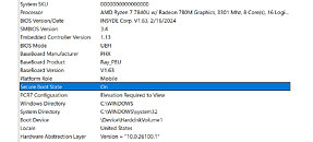
On your Windows PC, the Unified Extensible Firmware Interface (UEFI) firmware has a Secure Boot Certificate that mandates only verified software starts the boot-up sequence. Microsoft is preparing to refresh these certificates, and the company announced that millions of Windows PCs in circulation will receive new Secure Boot Certificates in an industry-wide gradual rollout to replace aging certificates that are expiring soon. According to the latest Windows Blog, the original Secure Boot Certificates introduced way back in 2011 are reaching the end of their planned lifecycle, with the expiration date set for late June 2026. This not only mandates updating but also requires a massive staged rollout from OEMs and Microsoft's partners to ensure that all Windows devices stay secure.

According to Microsoft, this is one of the largest industry collaborations that spans the Windows ecosystem, including servicing, firmware updates, and countless device configurations from OEMs and other hardware makers. Firmware makers are at the center with their UEFI BIOS patches, which will now have to replace their aging Secure Boot Certificates. The blog also states that OEMs have been provisioning updated certificates on their new devices, with some devices from 2024 and almost all PCs from 2025 updated to support the new certificate. Interestingly, older PCs and devices that were shipped prior to these years will also be taken care of, with major OEMs providing their own guidance on updating the certificate. If you don't see your OEM offering an update, be patient as the rollout is gradual.

SK hynix Plans 16 Gb LPDDR6 Modules Running at 14.4 Gbps, Samsung Chips Run at 12.8 Gbps

South Korean memory makers, SK hynix and Samsung, are preparing to showcase their next-generation LPDDR6 memory solutions at the International Solid-State Circuits Conference (ISSCC) 2026 in San Francisco, which will take place from February 15-19. As the premier event for showcasing advancements in silicon design, South Korean makers will present their best new technologies. For SK hynix and Samsung, this includes an update to their low-power DDR memory, now in its 6th generation. The LPDDR6 modules from SK hynix will arrive in 16 Gb capacities and offer a transfer rate per pin of 14.4 Gbps, built on the 1c generation (1Ξ³ generation) semiconductor node, which is the company's 6th generation of 10 nm DRAM. SK hynix runs these new modules at JEDEC's highest LPDDR6 speeds, meaning that the company is close to maxing out the new technology, and overclocked LPDDR6X versions might be arriving soon.

Samsung, on the other hand, has improved its LPDDR6 since the original CES 2026 presentation. The company will now present its 16 Gb LPDDR6 modules running at 12.8 Gbps, which is a significant improvement over the 10.7 Gbps modules from a few weeks ago. Samsung reportedly manufactures this LPDDR6 memory on a 12 nm process, which is slightly larger than SK hynix's 10 nm, but these modules also deliver great benefits. The company claims a 21% improvement in energy efficiency over its predecessor LPDDR5X. Additionally, Samsung's LPDDR6 memory uses NRZ signaling for I/O with a 12DQ subchannel, while SK hynix modules likely follow suit.

Amkor to Significantly Boost Arizona Packaging Capacity for Intel and TSMC

Amkor is preparing to greatly expand its Arizona-based operations, and the company will boost its spending not by a few percent, but by several multiples. The company is planning to triple its capital expenditures next year, with a dramatic increase from roughly $900 million in 2025 to as much as $3 billion in 2026, betting on massive demand from Intel and TSMC packaging technologies. This includes working with Intel and TSMC to enable their most advanced technologies like EMIB and CoWoS, all of which come in various form factors. We previously reported that Intel partnered with its long-time OSAT partner Amkor to take additional EMIB capacity that Intel's customers are interested in, in Incheon, South Korea.

However, as Amkor expands its facilities in Arizona, Intel will also collaborate with Amkor to deliver advanced EMIB packaging types on United States soil. While TSMC has been a primary choice for many high-density assemblies, growing interest in Intel's EMIB and Foveros options has led partners like MediaTek, Google, Qualcomm, and Tesla to consider alternatives. Interestingly, Amkor will also offload some of the CoWoS packaging work from TSMC by creating CoWoS packages on U.S. soil, instead of sending these chips back to TSMC's Taiwan fabs to finish production. Both CoWoS and EMIB/Foveros offer a list of benefits, making them highly sought-after packaging technologies for companies seeking to extract maximum performance from their chips. Amkor plans to be at the center of that supply chain and help Intel and TSMC handle more customers.

Xbox Game Pass and PC Game Pass Could Merge Into a Single Subscription

Microsoft is reportedly considering merging some of its subscription services into a single offering. According to The Verge, and later confirmed by sources from Windows Central, Microsoft is exploring the possibility of combining the PC Game Pass and Xbox Game Pass Premium subscription tiers into one "super" tier. This potential consolidation would address the increasingly complicated subscription lineup, which often confuses gamers and affects their subscription choices. Offering support for more than one platform in a single subscription could potentially revitalize the struggling subscription services sector at Xbox and align well with the timing of a new console release. The company is also looking into ways to incorporate more third-party service bundles into its Game Pass offerings.

Currently, PC Game Pass costs $16.49 per month after a significant price increase of nearly 40% last October, while the Xbox Game Pass Premium tier costs $15 but doesn't include the full library available to PC subscribers. At the top end is Xbox Game Pass Ultimate for $30 monthly, which offers day-one access to all Microsoft first-party releases, along with bundled perks from EA Play, Ubisoft+ Classics, and Fortnite Crew. Combining the PC and Premium tiers could simplify this structure, though it raises questions about pricing and feature access for current PC subscribers, or whether Microsoft will maintain the $16.49 price.

AMD "Medusa Halo" APU to Use LPDDR6 Memory

The next major refresh of AMD's Ryzen AI MAX APUs is still far away, but now we are putting together the pieces of the "Medusa Halo" APU puzzle. According to a famous leaker, @Olrak29_ on X, AMD's next-generation "Medusa Halo" APU will be complemented by LPDDR6 memory. This is one of the first LPDDR6 memory SoCs we are learning about, making it unique. Based on previous rumors, the silicon could have a 384-bit bus powering LPDDR6 memory, which would translate into massive bandwidth powering the SoC's new CPU and GPU configuration. This includes up to 24 "Zen 6" CPU cores and 48 RDNA 5/UDNA compute units for the GPU configuration. Paired with the added bandwidth from LPDDR6 memoryβ€”which these APUs greatly benefit fromβ€”"Medusa Halo" will be one of the best-performing SoCs when it launches.

Interestingly, memory manufacturers like Samsung and Innosilicon are already supplying LPDDR6 modules to customers for validation. Innosilicon's LPDDR6 modules boast an impressive speed of 14.4 Gbps, significantly faster than Samsung's initial modules, which achieve 10.7 Gbps. Innosilicon's modules offer a 1.5x increase in IO speed capability compared to the 9.6 Gbps of LPDDR5X previously available, along with improved efficiency. The latest LPDDR6 also increases the number of bits per byte of IO from 8 to 12. This results in LPDDR6's bandwidth at a single-channel 24-bit I/O speed being double that of LPDDR5X at a 16-bit single-channel. The company is reportedly collaborating with TSMC and Samsung to ensure sufficient production capacity for LPDDR6 IP, while Samsung relies on its own fabs for manufacturing memory.

Next-Generation Xbox is Windows 11 PC/Console Hybrid for Gaming and Productivity

Microsoft's next-generation Xbox console is reportedly taking an unconventional route by running on a customized version Windows 11 OS instead of the specialized console OS that typically powers these devices. According to Windows Central, the system will function essentially as a gaming PC that boots into an Xbox interface by default. This UI is likely similar to what the current Xbox Full Screen Experience looks and feels like, and will likely provide the same performance boost. We have already seen that Xbox FSE mode brings about a 9.3% reduction in RAM usage and about an 8.6% higher FPS due to the smaller system overhead. Users could exit that interface to access the full Windows 11 operating system, meaning the hardware would support Steam, EPIC, and other competing game stores, as well as standard PC applications alongside Xbox games.

This is Microsoft's first radical departure from the walled-garden approach that has defined console gaming for decades. What it could translate to is the first hybrid system that serves multiple purposes, from traditional gaming to running productivity suites of Microsoft 365 apps like Word, Excel, and others, all from the same system. Teams from the Windows and Xbox divisions are reportedly collaborating closely to adapt the operating system for living room use. Microsoft is also working with hardware partners like ASUS to create multiple devices at different price points rather than releasing a single standard console. Plans for a first-party handheld device are still under consideration, though the traditional console appears to be the main focus.

Intel Kills Pay-to-Use "Software Defined Silicon" Initiative

Intel has quietly deprecated its Software Defined Silicon initiative (SDSi), known as "Intel On Demand," according to a report from Phoronix. The company has archived the official GitHub repository for SDSi for Xeon, an effort intended to enable optional features on Intel's server processors that could be unlocked for an extra fee. Intel had hoped enterprises would pay to enable these features, but the initiative never gained mass traction and was only sporadically maintained. Because hyperscalers operate at massive scale, paying an additional fee to enable a feature on silicon they had already purchased made little sense, contributing to Intel's decision to abandon the project. Subscription services are similar in concept, but they generally apply to software on a monthly basis rather than one-time hardware activations.

Originally, Intel planned to make Quick Assist, Dynamic Load Balancer, and Data Streaming Accelerator available as On Demand features, alongside Software Guard Extensions and the In-Memory Analytics Accelerator. These were described on the Intel On Demand website as a "one-time activation of select CPU accelerators and security features." The Intel On Demand site has since been reworked to remove most information, leaving only a few documents and paragraphs. Thankfully, the idea of putting hardware features behind a paywall has not gained traction for now, leaving the paywall model to traditional software. At one point enthusiasts wondered whether Intel On Demand would trickle down to consumer CPUs, but with the project apparently dead, that possibility seems unlikely in the near term. Intel Upgrade Service existed in a similar format back in early 2010s, but was also short-lived.

AMD on FSR 4 for RDNA 3 and Older GPUs: "No Updates to Share at This Time."

AMD's FidelityFX Super Resolution 4 technology, now known simply as FSR 4, is currently supported in many games, but not across all AMD RDNA GPU generations. In response to an inquiry from Hardware Unboxed, AMD mentioned that it is still uncertain whether official FSR 4 support will be extended to the Radeon RX 7000 series and older GPUs, as the company reportedly has "no updates to share at this time." AMD official product separation stems from its RDNA 4 architecture and the support for 8-bit floating point instructions. While the latest RDNA 4 hardware supports Wave Matrix Multiply Accumulate in FP8 format, older RDNA generations like RDNA 3 and RDNA 2 lack this hardware instruction support and can't process 8-bit floating point data in this format.

However, older Radeon GPUs can instead rely on the 8-bit integer (INT8) data formats, which Radeon RX 7000 series fully supports. AMD accidentally leaked FSR 4 INT8 on its AMD GPUOpen platform, showing that FSR 4 on older GPUs is a possibility, which is just kept hidden for now. Later on, ComputerBase tested this leaked library, finding that FSR 4 offers a balance between native image quality and FSR 3.1 performance on both RDNA 3 and RDNA 2 hardware. In tests with Cyberpunk 2077 in 4K on Ultra settings using the AMD Radeon RX 7900 XTX, FSR 4 delivered 11% faster performance than native, but was 16% slower than FSR 3.1. Interestingly, performance may be the reason why AMD is holding these INT8 FPR 4 libraries back, but another point could be product separation.

30,000 NVIDIA Engineers Use Generative AI for 3x Higher Code Output

The company that started the entire wave of AI infrastructure and development is now enjoying the fruits of its work. NVIDIA has deployed generative AI tools across its company to an astonishing 30,000 engineers. In a partnership with San Francisco-based Anysphere Inc., the company is getting a customized version of the Cursor integrated developer environment, which focuses on AI code design. This is important to note as NVIDIA's engineers are now reportedly producing as much as three times the code compared to the previous development pipeline, and we are now probably using NVIDIA's products or services that have been designed by AI guided by humans.

NVIDIA offers a range of mission-critical products that cannot afford to be as error-prone as most AI-generated code tends to be. This includes GPU drivers that support everything from basic gaming to large-scale AI training and inference operations. The company is likely enforcing strict guidelines for its newly generated code, with an extensive range of tests required before the code is deployed in production. This isn't the first time NVIDIA has utilized AI-assisted workflows in its products. The company has already implemented a dedicated supercomputer that has been continuously enhancing DLSS (Deep Learning Super Sampling) for several years, and some chip designs have been optimized using the company's internal AI tools.

Intel Targets LPDDR5X-8533 for Core Ultra G3 "Panther Lake" Handheld Gaming Chips

In an exclusive report for VideoCardz, Intel is reportedly targeting an LPDDR5X memory speed of 8,533 MT/s for its upcoming Core Ultra G3 series of "Panther Lake" chips arriving in the second quarter for handheld gaming devices. After we learned that Intel is imposing certain memory mandates on its OEM partners, it seems like the Core Ultra G3 will face similar mandates from the company to prevent OEMs from "cutting corners" and implementing slower LPDDR5X memory. For the new handheld-tuned Core Ultra G3 and G3 Extreme, that specification is now set to 8,533 MT/s, which is slightly below its flagship "Panther Lake" Core Ultra X SKUs that can support LPDDR5X memory running at 9,600 MT/s.

Presumably, Intel will require OEM partners and makers of the next-generation handheld consoles to use this 8,533 MT/s memory on both SKUs. These chips will feature a 14-core CPU configuration, including two P-Cores, eight E-Cores, and four LPE-Cores. A key selling point of these SoCs is the Arc integrated graphics, with the G3 Extreme offering 12 Xe3 cores and the standard G3 featuring 10 Xe3 cores. The G3 Extreme plans to run the Arc B380 iGPU with 12 Xe3 cores at 2.3 GHz, just 200 MHz below the flagship Core Ultra X9 388H's Arc B390. Essentially, G3 Extreme handhelds can expect gaming performance similar to that of the flagship SKU, albeit with two fewer P-Cores and a slightly lower GPU clock speed. The regular G3 maintains its CPU capabilities, but the GPU is reduced to a 10-core Xe3 IP called Arc B360, with a GPU boost frequency of 2.2 GHz, resulting in a notable decrease in both gaming performance and TDP.

Report: Intel Cancels Flagship Core Ultra 9 290K Plus "Arrow Lake Refresh," But Keeps Other SKUs

Intel's "Arrow Lake Refresh" has not even been released, but the company has already canceled its flagship SKU planned for this refresh cycle, according to a report from VideoCardz. Two sources close to the media note that Intel's flagship Core Ultra 9 290K Plus might not roll out at all, despite the massive hype and leaked benchmarks indicating that Intel is releasing this CPU SKU as part of the "Arrow Lake Refresh" generation expected to arrive in March or April. Reportedly, Intel will instead focus on delivering value with its Core Ultra 7 270K Plus SKU, which carries 8 P-Cores and 16 E-Cores and a 5.5 GHz maximum turbo boost. For individual boosting frequency, P-Cores top out at 5.4 GHz, while the base runs at 3.7 GHz. For E-Cores, the boost frequency is set to a maximum of 4.7 GHz, while the base is set at 3.2 GHz.

As for a possible reason why Intel would cancel this SKU, the sources close to VideoCardz note that product overlap is the main issue, as the flagship Core Ultra 9 290K Plus would have the same core configuration as the Core Ultra 7 270K Plus, just with slightly higher clock speeds. Additionally, Intel already maintains a Core Ultra 9 285K SKU from the regular "Arrow Lake" family, meaning that the company would have three similar SKUs at the very top of the stack. This way, it would only have to maintain two products, which would simplify manufacturing and supply chain logistics, allowing Intel to spend more time preparing for the next-generation "Nova Lake" launch later this year.

AMD Ryzen Threadripper Pro 9995WX OC Draws 1,300 W Under Direct-Die Watercooling

AMD Ryzen Threadripper Pro 9995WX HEDT processor with 96 cores and 192 threads comes with a default TDP of 350 W. However, heavy overclocking can bring the CPU to 1,300 W and requires a custom integrated heat spreader (IHS) that serves as a direct-die waterblock. In the latest endeavor by Geekerwan, the enthusiast created a custom fin structure inside the Ryzen Threadripper Pro 9995WX IHS that serves as a direct-die waterblock to achieve an impressive overclock of 5.325 GHz, drawing an astonishing 1,340 W during load, with the entire system drawing around 1,700 W. According to Geekerwan, he contacted ASUS China regional manager Tony Yu to experiment with different IHS designs before "ruining" the IHS of a $12,000 HEDT CPU. He then proceeded with trying a straight fin structure common in commercial waterblocks, but also conducted computer simulations that showed a curved, wavy S-shaped fin structure is the most efficient in capturing heat, as the coolant flows over a longer distance with minimal obstruction, resulting in 20% better cooling than the straight fin structure.

The IHS of the AMD Ryzen Threadripper Pro 9995WX processor is 4.1 mm thick, which left Geekerwan with about 2.0 mm of fin depth and about 2.1 mm for the structural integrity of the IHS, which is subject to a lot of water pressure. After a heavy 19-hour session of CNC milling, the result is a CPU that ran between 30-50Β°C, which is an amazing temperature under Cinebench 2026 load. The system also placed 7th in Cinebench R23, just behind an LN2-cooled AMD Ryzen Threadripper Pro 7995WX running at 6.2 GHz. Impressive heat dissipation and the massive 5.325 GHz clock on a 96-core system are also made possible with an industrial chiller, two Bosch water pumps from cars, and a 37-gallon water tank. You can check out the entire process below.

MSI GeForce RTX 5090 Lightning Z GPU Listed at $5,200 in Taiwan

MSI's most powerful GPUβ€”the GeForce RTX 5090 Lightning Zβ€”will come with an extreme price tag to match, as the company has listed its GPU for NT$165,000, which works out to about $5,200. The company noted this pricing in a 24-hour giveaway scheduled to begin on Monday, February 9, at 10:00 AM Taiwanese time, lasting until Tuesday, February 10. The listing has revealed that the card we previewed at the 2026 International CES show is not only a premium design but also a premium-priced product, as the supply is limited to only 1,300 samples. MSI advertises a factory boost clock of 2,730 MHz and an "Extreme Performance" OC profile of 2,775 MHz. Additionally, the GPU is capable of reaching 3,742 MHz, which is the fastest LN2 GeForce RTX 5090 GPU ever.

The MSI GeForce RTX 5090 Lightning Z will come with an 800 W power limit out of the box, while the "Extreme" power preset mode gives it a 1000 W power envelope on the 360 mm AIO water cooling. The extensive engineering involved in the PCB design along with a 40-phase VRM allows the GPU to sustain multi-kilowatt loads. The card uses 28 Gbps Samsung GDDR7 memory, which can be overclocked to 36 Gbps on LN2. Additionally, only LN2 is capable of taming the XOC BIOS, which comes with 2.5 kW of power load and will require extensive PCB modifications. For a product that costs $5,200, only extreme overclockers would dare to modify the card. For the rest of us mere mortals, MSI recommends a power supply with a capacity of 1600 W, providing ample room for basic overclocking without ruining the card.

NVIDIA to Use SK hynix and Samsung HBM4 for "Vera Rubin" Without Micron

NVIDIA's upcoming "Vera Rubin" AI systems are scheduled for late summer shipping in the form of VR200 NVL72 rack-scale solutions that will power the next generation of AI models. However, not every memory maker of HBM4 qualified for a design win, as Micron has reportedly fallen out of the equation, with only Samsung and SK hynix left to supply the precious HBM4 memory. According to leaked institutional notes from SemiAnalysis, which tracks the supply chain in great detail, SK Hynix will represent about 70% of the HBM4 supply for VR200 NVL72 systems, with Samsung getting the remaining 30% of the supply. For a major memory maker like Micron, there is reportedly zero commitment for the supply of HBM4 memory.

Interestingly, this is not the end of Micron's share of memory in NVIDIA VR200 NVL72 systems. Instead of HBM4, the company will supply LPDDR5X memory for "Vera" CPUs, which can be equipped with up to 1.5 TB of LPDDR5X, making up for the lost share with the HBM4. It is possible that Micron didn't qualify for the significant system upgrade that NVIDIA performed for VR200 NVL72, which went from the initial system target of 13 TB/s in March 2025 to 20.5 TB/s in September. However, at CES 2026, NVIDIA confirmed that the VR200 NVL72 system is now operating at 22 TB/s of bandwidth, marking a nearly 70% increase in system bandwidth, all derived from aggressive memory specification scaling that the company demanded from the memory makers.

Major PC OEMs Reportedly Exploring Chinese CXMT Memory Amid Shortages

According to Nikkei Asia, some of the biggest PC makers like ASUS, Acer, Dell, and HP are exploring alternative memory suppliers amid industry-wide memory shortages, which are forcing PC OEMs to seek supply even from Chinese memory maker CXMT. Late last year, CXMT unveiled its homegrown DDR5-8000 and LPDDR5X-10667 memory modules at the 2025 China International Semiconductor Expo. This has likely prompted many OEMs to start finding alternatives to the traditional triad of SK Hynix, Samsung, and Micron, whose supply has been very limited outside AI accelerator workloads.

CXMT offers 12 Gb and 16 Gb LPDDR5X capacities, while DDR5 scales to 16 Gb and 24 Gb module formats. The 16 Gb DDR5 chips from CXMT measure 67 square millimeters, with a density of 0.239 Gb per square millimeter. The G4 DRAM cells are 20% smaller than CXMT's previous G3 generation. Reportedly, CXMT manufactures these chips using a 16 nm node, which is three years behind Samsung, SK Hynix, and Micron in manufacturing capabilities. However, CXMT is progressing quickly, and its DRAM modules adhere to the official JEDEC specifications and even exceeding the specification, making them ideal for OEM PCs depending on the use case.

Akasa Shows First Fanless Enclosures with LCD Screens

At Integrated Systems Europe (ISE) 2026 in Barcelona, Akasa showcased its latest solutions that embed LCD screens in passively-cooled cases. There are three versions, including "Kepler," "Maxwell Pro Plus," and "Euler CMX," all of which come with an LCD screen for monitoring or providing a visual interface that a user might need. First on the list is the new "Kepler" chassis, which is a 2U rack-mountable design with support for microATX and Mini-ITX boards, compatible with either Intel LGA1851 or LGA1700 sockets, capable of running anything from 12th to 14th Generation Intel Core processors, or Core Ultra in the latest 15th Generation "Arrow Lake." The system limits the CPU TDP to 35 W, which makes sense since it is a completely passively cooled enclosure. Kepler includes a 150 W AC-to-DC converter to power the system, and there is the possibility to install up to four single-slot low-profile PCIe cards or anything that fits within four slots of low-profile PCIe space.

NVIDIA Confirms Dynamic Multi-Frame Generation and 6x Mode Arrive in April

According to HardwareLuxx, NVIDIA has confirmed that Dynamic Multi Frame Generation (MFG) and Multi Frame Generation 6x mode are scheduled for release in April. HardwareLuxx visited NVIDIA's Munich office in Germany and obtained some exclusive information from the company. This includes the exact release date for NVIDIA's latest Dynamic Multi Frame Generation and Multi Frame Generation 6x mode, which are bringing NVIDIA DLSS 4.5 technologies to the public. With DLSS 4.5, NVIDIA can get the GPU to draw up to 5 frames following each traditionally rendered frame, made entirely using generative AI. Using the new MFG 6x mode results in a 6x performance uplift, where a game that traditionally runs at 60 FPS can now run at 360 FPS.

However, for setups where a monitor is maxed out at 240 Hz or 144 Hz, like many gaming panels are, using 6x MFG would be overkill. This is where Dynamic MFG comes into play. This technology will determine which MFG multiplier is needed based on the display's refresh rate capability that is used for the MFG target and the input framerate from the upscaler. The company calls this "automatic transmission" for MFG, making a parallel to modern vehicle automatic transmission systems that also switch gears based on the need. For example, in demanding game scenarios, the MFG multiplier could be 4x, 5x, or 6x, while less demanding game sections like the settings menu or some static scenes will require only a 2x multiplier to achieve the FPS goal. HardwareLuxx tested this and reported smooth transitions while keeping the FPS stable.

Corsair Stock Falls Below $5 Ahead of Earnings

Corsair has been listed on Nasdaq since September 2020, when the company made an IPO at $17 per share. However, the company, which is a gaming staple, has now fallen to a measly sub-$5 range for the first time. Just days ahead of its full-year earnings and Q4 2025 results scheduled for February 12, Corsair is trading at $4.80 with a market capitalization of $504.63 million. During the first three months of its public listing, the stock reached an all-time high of $51.37, and the price has been in free fall since. This represents a 90% market value reduction over nearly five and a half years.

For the previous Q3 2025 report, the company reported a year-over-year revenue increase of 14% to $345.8 million, with projections for a full-year outlook being $1.425 billion to $1.475 billion, and adjusted operating income in the range of $76 million to $81 million. However, since the stock is now falling, we can expect that the earnings will possibly be at the lower end of the range. Interestingly, Corsair is one of the few publicly listed companies with revenues exceeding its market capitalization. This indicates that the company is capturing a significant revenue share among PC enthusiasts, but its operating costs are very high, and the business is net profit margin negative, which is a massive concern for investors using their hard-earned funds.

No NVIDIA GeForce RTX 50 "SUPER" GPUs This Year, RTX 60-Series Also Pushed Back

Artificial Intelligence may be eating the world of software now, but gamers are suffering. According to The Information, NVIDIA has reportedly entirely postponed the launch of its GeForce RTX 50 "SUPER" refresh, as the company's executives are prioritizing AI accelerators over the gaming sector, which consumes precious cutting edge GDDR7 memory. The GeForce RTX 50 "SUPER" refresh was originally scheduled for an announcement at CES 2026, with shipping in Q1 or Q2 of 2026. However, the GDDR7 memory used in the SUPER lineup was a high-capacity 3 GB version, which NVIDIA managers in December deemed too important for gamers, postponing the refresh entirely.

The "SUPER" series was planned with denser GDDR7 memory modules, offering 3 GB of capacity per chip, increasing the memory configuration of the standard GeForce RTX 5070, RTX 5070 Ti, and RTX 5080. Initially, the RTX 5070 SUPER was planned with an upgrade to offer 18 GB, while the RTX 5070 Ti SUPER and RTX 5080 SUPER would each provide 24 GB of GDDR7 memory. As NVIDIA's AI GPU portfolio also uses the high-density GDDR7 memory, like the RTX PRO 6000 "Blackwell" and "Rubin CPX" the company has decided to instead prioritize this high-margin business, leaving gamers with inflated prices of the regular GeForce RTX 50-series.

Intel Core Ultra G3 "Panther Lake" Handheld Gaming Chips to Come in Q2 of 2026

When Intel unveiled its "Panther Lake" Core Ultra Series 3 mobile processors built on the 18A node, the company announced that a separate version fine-tuned for handheld gaming consoles is in the works. Called Intel Core Ultra G3 "Panther Lake," the chip is now scheduled to arrive in the second quarter of 2026, according to Golden Pig Upgrade. The company plans to bring two SKUs to the masses, which will be called G3 and G3 Extreme, each carrying a 14-core CPU configuration consisting of two P-Cores, eight E-Cores, and four additional LPE-Cores. However, the real star of the show of this SoC will be the Arc integrated graphics, which will arrive with 12 Xe3 cores in the G3 Extreme, or 10 Xe3 cores in the regular G3.

For the G3 Extreme, the plan is to run the Arc B380 iGPU with 12 Xe3 cores at 2.3 GHz, which is just 200 MHz shy of the flagship Core Ultra X9 388H's Arc B390. Basically, G3 Extreme handhelds can expect similar gaming performance to what we observed in our review of the flagship SKU, just with two P-Cores less and a slightly lower GPU clock. For the regular G3, the CPU configuration retains its capability, but the GPU drops to a 10-Core Xe3 IP called Arc B360. This integrated graphics drops core counts and GPU boost frequency to 2.2 GHz, which will result in a significant reduction in both gaming performance and TDP. Intel still hasn't revealed plans about TDP configurations, so we have to wait a bit longer for that.

Intel Confirms "Nova Lake-P" Features Xe3P-LPG Graphics

In the latest set of enablement patches, Intel has confirmed that the upcoming "Nova Lake-P" processors will utilize Xe3P-LPG to power their integrated graphics. In addition, "Nova Lake-P" processors will include multiple new IPs like the Xe3P-LPM for media processing, which includes decoding and encoding, and the Xe3P-LPD for display output processing. These new IPs will work in tandem to deliver the next generation of Intel graphics, which will be separated into two categories within the "Nova Lake" generation. Interestingly, we learned a while back that not every "Nova Lake" SKU will ship with the same GPU configuration. "Nova Lake-H" mobile variants are expected to support ray tracing with the Xe3P-LPG graphics, while "Nova Lake-S," "Nova Lake-HX," and "Nova Lake-UL" may not.

The company seems to be selectively enabling advanced GPU features across these SKUs rather than providing a uniform feature set, as Xe3P-boosted "Nova Lake-H" notebook chips will be succeeding "Panther Lake-H" with its Xe3 GPU IP, so the new P variant will bring more power to mobile gaming setups and be a true successor in late 2026 or early 2027. This type of segmentation is a common strategy to differentiate products using the same silicon, which will influence purchasing decisions for gamers, creators, and laptop buyers of the future "Nova Lake" systems. Additionally, bundling next-generation GPU graphics IP like the Xe3P-LPG will be of massive significance only to those users relying on integrated GPUs, while those purchasing systems with discrete GPUs will focus primarily on the CPU and display/media output side.

Tenstorrent Cuts 20 Cores From Already-Shipping "Blackhole" P150 Cards

Tenstorrent, a startup focused on designing high-performance AI accelerators and led by the renowned computer architect Jim Keller as CEO, has announced significant hardware updates to its existing Blackhole P150 accelerators, which include the P150a and P150b models. In the latest documentation change, the company notes that its Blackhole P150 accelerators will now work with about 14.3% fewer cores than originally advertised. In the official documents, the P150 accelerators are now shipping with 120 working "Tensix" cores instead of the previously advertised 140 cores. The reason for this change is unknown, as the company provided a vague explanation: "To present a unified interface to metal and other system software, firmware v19.5.0 and later will change the core count on all existing cards to 120. Typical workloads show a non-material (~1-2%) performance difference."

The Blackhole P150 accelerators featured 140 "Tensix" cores and 32 GB of GDDR6 memory, operating at up to 300 W in an actively cooled form factor designed for desktop workstations, and the P150a model includes four passive QSFP-DD 800G ports. However, as the number of cores is reduced by approximately 14%, TeraFLOPS take a nosedive as well. In the older documents for the 140-core SKUs, the BLOCKFP8 8-bit floating point performance was listed at 774 TeraFLOPS, while the new 120-core version reduces that number to 664 TeraFLOPS at the same precision level. Why this sudden change is happening is still a mystery. However, the HPC community with a lot of knowledge in the industry suggests a few reasons.

Intel CPUs Record First Period of Growth on Steam Survey After Months of Decline

As February has just started, Valve finished processing data for the January edition of the Steam Hardware and Software Survey. One of the few interesting takeaways is that for the first time in months, Intel's share of consumer CPU usage has seen an uptick, instead of the slow decline it has been experiencing. According to the January update, Intel's CPU share among Steam platform users has grown to 56.64%, representing a small but pleasant increase of 0.25% over the December data. On the other hand, AMD recorded a slight decrease of 0.19%, now standing at 43.34% of the market. This means that Intel's market share has increased for the first time in months, as data from September reported a market share of 58.61%, then October showed 57.82%, 57.30% in November, and 56.39% in December. The chain of declining share has finally stopped, suggesting that Intel could have a chance to rebound in the consumer market section.

On the contrary, AMD's CPU market share has been rising for months, moving up from 41.31% in September to 43.53% in December, with a small correction now standing at 43.34%. This indicates that many new CPU purchasing decisions were made in favor of AMD, driven by the massive popularity of its Ryzen 9000X3D series, which has been well-received by PC enthusiasts. In contrast, Intel's latest "Arrow Lake" launch has faced some initial challenges with less-than-expected gaming performance, but besides discounts and firmware updates improving the situation, the community is now anticipating the launch of the "Arrow Lake Refresh" scheduled for March or April, which is expected to address these issues by shipping with higher out-of-the-box frequencies and additional tuning.

AMD Confirms Steam Machine in Early 2026, Xbox SoC Powered by RDNA 5 in 2027

AMD posted its record fourth quarter revenue of $10.3 billion in 2025, and during the earnings call, the company issued some guidance on the upcoming product portfolio. During the call, AMD confirmed that Valve's Steam Machine is on track and shipping early this year, while its custom SoC division that designs processors for PlayStation and Xbox consoles will deliver an RDNA 5-based SoC for the next-generation Xbox console. While the Steam Machine specifications are confirmed, Xbox "Magnus" SoC is still largely a collection of rumored specifications. The "Magnus" SoC is rumored to feature the largest APU ever designed for a consumer console, with a 408 mmΒ² chiplet design. Of this, 144 mmΒ² is dedicated to the SoC built on TSMC's N3P node, while the GPU occupies 264 mmΒ². The AMD chip is expected to include up to 11 CPU coresβ€”three Zen 6 and eight Zen 6cβ€”alongside a substantial GPU setup with 68 RDNA 5 compute units, four shader engines, and at least 24 MB of L2 cache. Memory might expand to 48 GB of GDDR7 on a 192-bit bus. A dedicated NPU is rumored to offer significant on-device AI performance, with reports suggesting up to 110 TOPS.
Dr. Lisa SuFor 2026, we expect semi-custom SoC annual revenue to decline by a significant double-digit percentage as we enter the seventh year of what has been a very strong console cycle. From a product standpoint, Valve is on track to begin shipping its AMD-powered Steam Machine early this year, and development of Microsoft's next-gen Xbox featuring an AMD semi-custom SoC is progressing well to support a launch in 2027.

Western Digital Designs High-Bandwidth HDDs That Quadruple I/O Speeds

Western Digital has today presented its latest effort to catch up with traditional QLC NAND Flash SSDs by improving its HDD offerings. With the latest High-Bandwidth HDDs, Western Digital has implemented two new technologies in a classical multi-platter HDD design. The first innovation comes in a form of High Bandwidth Drive Technology, which enables double the I/O bandwidth with a path to 8x the current bandwidth in the future. It relies on simultaneous reading and writing from multiple heads on multiple tracks, which is already in customer hands for validation. The second one is Dual Pivot Technology that introduces a second set of independent actuators on a separate pivot, which will not scarify drive capacity unlike older dual actuator designs.

Using Dual Pivot Technology, HDDs can pack more drive platters in a standard 3.5-inch body for higher capacities, and the performance grows by an additional 2x, which is 4x I/O bandwidth compared to today's drives. This technology will pave the way for 100 TB HDDs, that offer speeds comparable to QLC-based SATA III SSDs, at much better price/performance ratio and better data retention, prompting the massive boom of HDD development. Western Digital's drives with High Bandwidth Drive Technology are already shipping to customers, while drives with Dual Pivot Technology are in development in Western Digital's labs and are scheduled to become available in 2028, with early customer sampling probably much sooner.

AMD Radeon AIBs to Prioritize 8 GB GPU SKUs and Push 10% Price Hike

According to Chinese Board Channels, a reliable source of GPU news, AMD's add-in board (AIB) partners are preparing for another round of GPU price increases. They also seem to be shifting their product focus toward 8 GB Radeon models. After distributors implemented a 5-10% price adjustment in January, another increase is reportedly planned for February or March, though the exact percentage is not yet known. Board Channels also reports that AMD is expected to prioritize stocking 8 GB SKUs such as the Radeon RX 9060 XT 8 GB and the older RDNA 3-based RX 7650 GRE, rather than the 16 GB SKUs like the Radeon RX 9070 XT. This shift is due to a shortage of GDDR6 memory, which is reducing the profit margins for AIBs without a significant price increase.

Distributors reportedly stocked up after January's price increase, which could lead to uneven availability if resellers hold onto inventory in anticipation of another adjustment. With DRAM prices having risen sharply in recent months, manufacturers are reassessing which memory configurations to produce, favoring 8 GB variants because they are cheaper to manufacture. This shift might also cause some 16 GB parts to become more expensive, narrowing the price gap between AMD and NVIDIA in the midrange market. The earliest effects of these changes are expected to be seen in mainland China, where partners may allocate more volume to 8 GB cards and reduce the output of certain 16 GB GRE and non-GRE models. We are yet to see how it reflects on the Western stores and pricing imposed by retailers like Amazon, Newegg, and others.

Firefox 148 Gets AI Killswitch After a Massive Community Backlash

Mozilla's plans to make Firefox "a modern AI browser" have fallen flat on its face. When Anthony Enzor-DeMeo took over the Mozilla the new CEO, he announced plans to make the browser a modernized version of AI-first browsing experience. However, massive community backslash has resulted in the CEO quickly apologizing to the community and promising a killswitch. In the upcoming Firefox version 148, scheduled for a release on February 24, there will be an option to turn off AI features in the browser individually, or all at once. This includes AI-assisted translations, alt text in PDFs, AI-enhanced tab grouping, link previews, and an AI chatbot in the sidebar. Users can choose which features to enable or disable, and those who prefer not to use any AI functions can turn them off entirely with a single switch. This setting will persist even after future updates, ensuring that users who opt out will not encounter generative AI features.

Mozilla is fulfilling its earlier promise to implement an AI killswitch, an option increasingly sought after by many users. While some enjoy a web experience assisted by AI, many do not. Having an option to individually turn off specific features, or all at once, is the perfect solution. Interestingly, this is not the first time we are seeing features from companies that are marked as new updates, but instead delivering a shield from all the "AI enhancements." Users are clearly expressing a frustration of AI everywhere approach, and Mozilla is aiming to position Firefox right where the community wants it to be. For Firefox Nightly users, the feature is available right away. However, for Firefox stable, users must wait a few days until February 24 to install Firefox 148.

Intel Core Ultra 5 250KF Plus "Arrow Lake Refresh" Listed by Romanian Retailer

Intel's upcoming "Arrow Lake Refresh" are weeks away from the final release, but new listing suggests that there might be more SKUs getting a refresh makeover than we initially thought. In the latest listing by a Romanian retailer, there is a new SKU called Core Ultra 5 250KF Plus, with a code number BX80768250KF. The SKU is supposed to be the first version of the ARLR family with a "KF" mark, meaning that there won't be an integrated GPU in this processor Instead, only the CPU is provided, meaning that a GPU is mandatory, much like the previous KF SKUs. In the listing there is a mention of 4.2 GHz frequency, which aligns with the previously rumored Core Ultra 5 250K Plus and its P-core base speed of 4.2 GHz. This means that other specifications will remain similar to the Core Ultra 5 250K Plus, like the E-Core base speed of 3.5 GHz, E-Core turbo of 4.7 GHz, and P-Core boost frequency of 5.3 GHz. The only difference will be the lack of iGPU, as it has been a case with previous KF SKUs.

Interestingly, the Romanian retailer is also listing the Core Ultra 250K Plus (BX80768250K) and Core Ultra 270K Plus (BX80768270K), while the flagship Ultra 9 290K Plus is not yet listed. This doesn't necessarily mean the SKU won't exist, but rather that this preliminary listing is incomplete for now. For the Core Ultra 5 250KF Plus, the retailer listed it at 1,049 Romanian Leu, which is about $243. As previous leaks suggest a March or April release of the ARLR family, we can expect the information and listings to intensify in the coming weeks. Some early benchmark runs also point to a 10% performance boost in flagship SKUs with the new refresh, so we have to wait and see how these mid-range chips perform in more testing.

Nintendo Switch Family Surpasses 155 Million Units Sold

Nintendo's return to the modern handheld gaming market has proven to be a record-breaking success. The company has reportedly sold 155 million Switch units worldwide since its initial launch. The latest Nintendo Switch 2 has sold 17.37 million units since its release in June 2025. During the holiday quarter, shipments reached 7.01 million units globally, while the original Switch sold 1.36 million units in the same period. Combined lifetime shipments for the Switch family now stands at 155.37 million units, surpassing the Nintendo DS total of 154.02 million, making it Nintendo's best-selling console ever.

Regarding software for these record-breaking units, sales for the new console are also strong, with 37.93 million Switch 2 titles sold to date, largely driven by first-party games. Mario Kart World has reached 14.03 million copies, Donkey Kong Bananza 4.25 million, and PokΓ©mon Legends: ZA 3.89 million. Kirby Air Riders, released in November, has sold 1.76 million units. The older Switch remains commercially relevant, with cumulative software sales of 108.93 million this quarter. Long-running catalog titles such as Mario Kart 8 Deluxe, now at 70.59 million copies, and Super Mario Party Jamboree at 9.41 million, continue to sell well, aided by backward compatibility.

OCCT Tool Gets Intel Xeon 600 "Granite Rapids-WS" Overclocking Support

OCBASE has updated its OCCT tool to include overclocking support for Intel's latest Xeon 600 "Granite Rapids-WS" workstation processors, designed for precise tuning of Intel's best HEDT offering. While OCCT is traditionally known for hardware stability testing, OCBASE aims to transform it into a universal platform that combines fine-tuning, including overclocking, with stability testing in a single application. The company has worked with Intel to create a special skin for the OCCT tool, featuring an Intel-like blue and white theme. Besides the visual makeover, lots of under the hood changes follow.

For instance, Intel's flagship Xeon 698X, with 86 cores and 172 threads and 336 MB of L3 cache, can be overclocked from the application UI. The processor operates at a 2.0 GHz base clock and can boost up to 4.8 GHz with Turbo Boost Max 3.0 or 4.6 GHz with Turbo Boost 2.0. Intel confirms that the 698X is fully unlocked, which is unusual for the Xeon processor family. With OCCT, users can now make per-core clock adjustments and live parameter edits while running continuous stress tests. Currently in a closed beta program, the public release is expected within weeks and will include Linux compatibility.

Loongson 3B6000 Benchmarked, Only Delivers a Third of AMD Ryzen 5 9600X Performance

Chinese company Loongson has been developing custom processors based on the LoongArch instruction set, a new design initiated in 2020. Phoronix reviewed the company's 3B6000 processor, which has 12 cores supporting simultaneous multithreading (SMT2), resulting in 24 threads. The platform is compatible with DDR4 memory, with a controller targeting speeds up to 3,200 MT/s and ECC support, and the CPU runs at 2.4/2.5 GHz base frequency. In testing, the 3B6000 processor achieved about one-third the performance of the AMD Ryzen 5 9600X in aggregate benchmark testing. However, it outperformed the Raspberry Pi 500+ by a factor of 2.5, placing it between single-board computers and entry-level desktop systems.

For testing, Phoronix used the 3B6000x1-7A2000x1-EVB evaluation board, which appears dated compared to current motherboard designs, especially in terms of component selection and the cooling solution for the chipset. Expansion options include two PCIe x16 slots, one PCIe x4 slot, an M.2 connector, and four SATA ports. The integrated graphics unit supports both HDMI and VGA outputs. While the LoongArch64 architecture represents China's effort to develop an independent instruction set with the ability to tune features like security and specialized workloads, these benchmarks suggest the hardware execution still lags several generations behind x86-64 designs from AMD and Intel. Significant, multifold improvements are needed before it can match the performance of Western CPU makers.

Intel's Core Ultra 9 290K Plus Shows 10% Performance Boost Over Core Ultra 9 285K

Intel's next desktop "Arrow Lake Refresh" CPU upgrade is inching closer to reality. The Core Ultra 9 290K Plus has been spotted in a new Geekbench run, adding to the evidence that the "Arrow Lake Refresh" will indeed offer a meaningful performance improvements over its predecessors. The test system used an ASUS ROG Strix Z890-E Gaming Wi-Fi board with 64 GB of DDR5-6800 memory. The processor achieved scores of 3,535 in the single-core test and 25,106 in the multicore test. Compared to the Core Ultra 9 285K's typical scores of around 3,200 and 22,560, this represents improvements of approximately 10.5% and 11.3%, respectively. These results place the 290K Plus at the top of Intel's consumer CPU rankings in Geekbench's database. An earlier leak on different hardware showed slightly lower results, suggesting that this newer test run benefits from better optimization rather than just faster memory.

The 290K Plus SKU keeps the same 24-core layout as its predecessor with 8 P-Cores and 16 E-Cores, plus identical power limits of PL1 of 125 W and PL2 of 250 W. The gains come from higher clock speeds. According to rumors, the efficiency cores now boost to 4.8 GHz, up 200 MHz, while the performance cores get an extra 100 MHz on both turbo and thermal velocity boost. The benchmark registered the chip running at 5.7 GHz during testing. Intel has confirmed the ARLR is coming but has stayed quiet on specific models and dates. Leaks suggest a March or April release, and since these chips use the same LGA 1851 socket, they should work as drop-in upgrades for current Z890 motherboards. As with any pre-release numbers, may not reflect final CPU performance, so final performance data and gaming results that come from third-party reviews will show the real-world situation.

(PR) Arm Flexible Access Helps Startups Build Chips Faster

Arm Flexible Access is evolving, unlocking broader startup eligibility, expanded edge AI capabilities, and a more flexible way to design, test, and bring silicon to market. Innovation in silicon design thrives on iteration. For startups and established design teams alike, the ability to explore, test, and refine without financial friction is essential. That's why Arm Flexible Access is evolving to make that journey even easier.

Arm Flexible Access already offers up-front, low-cost or no-cost access to a wide portfolio of Arm technology, tools, and training. This "try before you buy" model allows teams to build and test designs freely, only paying licensing fees for the technologies used in production silicon. It's helped launch over 400 chips across more than 100 companies.

Intel Mandates 7,467 MT/s+ Memory for "Panther Lake" Arc B390/B370 Integrated Graphics

Intel is reportedly mandating OEM integrators of the latest "Panther Lake" SoCs to use LPDDR5X memory starting at 7,467 MT/s and beyond, with an interesting software differentiator between adequate speeds or those below. According to Golden Pig Upgrade, LDDR5X memory running below the 7,467 MT/s threshold will force the software to display a generic mark of "Intel (R) Graphics," while configurations with that exact memory speed or higher will display the full name of "Intel (R) Arc (TM) Graphics B390" or "Intel (R) Arc (TM) Graphics B370" marking in Windows 11 Task Manager. Reportedly, Intel is doing this to stop OEMs from cutting corners with their "Panther Lake" laptop configurations, where they could bundle a lower-speed LDDR5X memory out of the Intel specification.

Without the required memory, Intel's Arc B390/B370 iGPUs would likely be left starving for bandwidth, as the whole SoC is being powered by that memory. At higher speeds, memory can do the data transfer faster, resulting in a boost of the overall system performance, and most importantly, the frame rate that these chips can push out. Especially for single-package systems like "Panther Lake" is, faster memory is a great way to get extra performance boost. Intel's flagship SKUs are advertised as capable of running with LPDDR5X memory at speeds up to 9,600 MT/s, which is just below the point where LPDDR5X technology tops out at 10,700 MT/s. Interestingly, there are lots of options from Intel's OEM partners that integrate top-end memory, which is a positive sign for the ecosystem.

Intel XeSS 3 Runs on Arc B580 Before Official Support Lands

Intel XeSS 3 with multi-frame generation (MFG) is expected to be available this month for the Arc B580 "Battlemage" graphics cards. However, some Redditors suggest there's a workaround to enable XeSS 3 and gain the FPS boost from MFG through a simple file swap. Gamers using Intel's Arc B580 have discovered that by installing Intel's driver package for "Panther Lake"β€”which includes XeSS 3 with MFGβ€”and renaming certain dynamic link libraries, the drivers for Arc B580 can use libraries intended for Arc B390 and Arc B370 integrated graphics. The process is straightforward, allowing gamers to download, extract, rename, and activate XeSS 3 on their non-PTL systems without issues. This raises the question of why Intel chose not to officially support the discrete "Battlemage" GPUs for XeSS 3 on the new driver release day. Possible reasons could include marketing strategies or additional beta-testing before the official release.
Here is a complete step-by-step solution.

Microsoft Steps Back from "AI Everywhere" in Windows 11 to Focus on Core Features

If you're tired of seeing Microsoft's AI features like Copilot, agentic workloads, and Recall forced into their products, you're not alone. Microsoft has finally confirmed that it will be stepping back from its "AI everywhere" strategy. According to an exclusive report by Windows Central, the internal Windows 11 teams at Microsoft are now focusing on reducing forced AI integration. Instead, they aim to address what truly matters to consumers, such as fixing the bug-prone operating system and enhancing core features for a smoother user experience. The integration of Copilot into basic apps like Notepad and Paint is reportedly under review, and Microsoft may remove these features to restore the basic functionality users have come to appreciate. This includes features like basic text formatting and tables in Notepad, which are nice additions to a core application.

Additionally, forcing Copilot AI button in every application has been paused, as there has been very little interest from users in actually using these features. TechPowerUp Forums has been a constant source of criticism for Microsoft's forced AI integration, among the remaining large crowd of PC enthusiasts who have been fighting the "AI everywhere" approach for a while. Microsoft's telemetry records usage of these AI buttons and additions, likely showing that only a few percent of Windows 11 users are actually interested in having AI access every application layer, especially with the recent ambition to shape Windows 11 into "agentic OS." The company confirmed that these features are a security nightmare to maintain, so thankfully these efforts are now cancelled.

AI Arms Race Targets Google TPUs as DOJ Charges Ex-Googler with Espionage

The AI arms race is now in full swing, and corporate espionage is reaching levels beyond what we previously imagined. According to the United States Department of Justice (DOJ), former Google software engineer Linwei Ding has been convicted of economic espionage and theft of confidential AI technology, specifically related to Google Tensor Processing Units (TPUs). An FBI investigation revealed that the ex-Googler was suspected of stealing information about the entire infrastructure surrounding TPUs, including chip architecture, external connectivity, and more. The DOJ concluded that Linwei Ding was acting for the benefit of the People's Republic of China (PRC), with the primary goal of stealing sensitive intellectual property that Google has spent years and billions of US Dollars developing. Naturally, Google collaborated with the FBI to protect its intellectual property and found the former employee guilty of stealing as many as two thousand pages of confidential information.
U.S. Department of JusticeThe trade secrets contained detailed information about the architecture and functionality of Google's custom Tensor Processing Unit chips and systems and Google's Graphics Processing Unit systems, the software that allows the chips to communicate and execute tasks, and the software that orchestrates thousands of chips into a supercomputer capable of training and executing cutting-edge AI workloads. The trade secrets also pertained to Google's custom-designed SmartNIC, a type of network interface card used to facilitate high speed communication within Google's AI supercomputers and cloud networking products.
❌