Reading view

Framework DDR5 Memory Costs $12-16 per GB of Capacity with Another Price Hike

Laptop and Mini-PC maker Framework is sharing another update with the community about the company's cost base for acquiring DRAM, such as DDR5 memory. In its latest February update, the company notes that the cost for DDR5 memory in its systems is now priced at $12-16 per GB of capacity, depending on the kit size and total capacity. This means that for a 16 GB kit, customers are expected to pay anywhere between $192-256, and as much as about $400 for 32 GB of DDR5 memory in its Laptop 12/13/16 models. According to the company blog post, this represents an average price that Framework is charging depending on the kit, as there is different pricing for a single higher-capacity sticks or dual lower-capacity DIMMs going into the system.

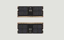
In late December 2025, we reported that Framework's pricing was $10 per GB for 8 GB, 16 GB, and 32 GB modules, and a bit higher for dual rank non-binary 48 GB modules. However, just two months later, the situation is now much worse, as we are seeing Framework's suppliers increasing memory costs anywhere from 20-60%, depending on the configuration.

PlayStation UK Now Offers PS5 Leasing Starting at £9.95 per Month

Console gamers might not necessarily become console owners, as Sony's PlayStation UK division is experimenting with leasing the PlayStation 5. The lease starts at £9.95 per month and varies depending on the console version. This plan involves a 36-month lease for a PlayStation 5 Digital Edition with 825 GB of storage. Opting for a shorter lease, such as 24 months or 12 months, increases the monthly cost to £10.49 and £14.59, respectively. Other versions of the PlayStation 5, like the PlayStation 5 Pro, as well as accessories such as the DualSense Edge Wireless Controller, PlayStation VR2, and PlayStation Portal Remote Player, can also be leased for an additional cost per month, based on your lease choice. There is also a "rolling" lease option where users pay £19.49 monthly and can cancel at any time, provided they return the console.

A quick calculation shows that the 36-month lease is the most expensive, totaling £358.20 by the end of the term. Afterward, users have several options: upgrade the console by returning the old one, continue with the monthly subscription, or exit the Flex plan by returning the console. For the 24-month and 12-month plans, users pay £251.76 and £175.08, respectively, by the end of the lease period. These plans also offer the same options: return the console, upgrade the hardware and return, or continue paying the monthly fee for a while longer. The only flexible plan is the monthly rolling option, which allows users to pay £19.49 per month without any long-term commitment, and they can cancel at any time. This plan doesn't require any upfront payment for the console.

Report: AMD Breaks 40% Server Revenue Share for the First Time

It is official: AMD is now capturing 40% of the entire server CPU market revenue share, according to data from Mercury Research. In the final quarter of 2025, AMD EPYC server CPUs managed to capture 41.3% of the revenue in the server/data center market that hyperscalers are spending on. This is a 1.8% increase from Q3 2025 and an impressive 4.9% year-over-year growth in a multi-billion USD data center market. For unit share shipment, AMD now stands at 28.8%, meaning the company is actually selling more SKUs at a higher average selling price. Intel, on the other hand, now holds 71.2% of the unit share while capturing 58.7% of the revenue share, indicating that Intel Xeon processors are now selling for a lower ASP with more units needed to reach this revenue.

The situation in the desktop segment looks interesting as well, with AMD's revenue share in the desktop CPU market now at 42.6%, while the unit share is at 36.4%. Again, this means that AMD's Ryzen processors sell at a higher ASP, nearly capturing half of the desktop CPU revenue with a bit more than a third of the unit sales. This sector also grew 1.6% sequentially, while Ryzen CPUs won the hearts of 14.6% more gamers for a yearly revenue share increase.

NVIDIA App Hotfix 11.0.6.386 Fixes Optimus MUX Switching Issues

NVIDIA released a hotfix version 11.0.6.386 for its app that addresses a serious issue where users were unable to access advanced Optimus MUX switch options. These options were reportedly grayed out during random MUX switch scenarios. As a reminder, NVIDIA Optimus technology is designed to switch between integrated and dedicated graphics within the system to conserve power. This feature is not used on desktop systems but on laptop PCs that have an iGPU from an Intel or AMD processor and a dedicated NVIDIA GeForce GPU. During light workloads, such as basic image display, the iGPU is used, which saves laptop battery due to its low power consumption. However, when demanding graphics tasks are running, NVIDIA uses a MUX switch to activate its dedicated GPU for heavier workloads. In the previous NVIDIA app version, users reported that some advanced Optimus MUX switch options were "grayed out" during random MUX switch scenarios. The issue has now been isolated, and users can either update the NVIDIA app from the software itself or download it from the link below, which is a direct link to NVIDIA's .exe file.

DOWNLOAD: NVIDIA App Hotfix 11.0.6.386

Intel Arc B390 Achieves 12x Performance and 8x Performance-per-Watt vs Gen9 iGPU

Intel's 10 years of integrated graphics have yielded massive performance improvements, according to recent testing by Phoronix. The latest testing shows that moving from Intel Gen 9 integrated graphics in the "Kaby Lake" CPUs introduced in 2016 to the modern Intel Arc B390 with Xe3 cores in "Panther Lake," results in a 12x performance boost and a 8x performance-per-watt efficiency increase. This is remarkable progress for Intel's iGPU team, delivering steady performance improvements year-over-year, with a significant boost in recent years. Phoronix tested iGPUs of top-end Core models, including: Core i7 8550U "Kaby Lake," Core i7 8565U "Whiskey Lake," Core i7 1065G7 "Ice Lake," Core i7 1185G7 "Tiger Lake," Core i7 1280P "Alder Lake," Core Ultra 7 155H "Meteor Lake," Core Ultra 7 258V "Lunar Lake," and finally the Core Ultra X7 358H "Panther Lake" processor.

The oldest among these is the "Kaby Lake" generation, which utilized Intel UHD Graphics 620 on Gen 9 architecture, while the newest is Intel's most powerful creation to date—Arc B390 based on Xe3 cores. Comparing the 14 nm FinFET Intel node to the TSMC N3E node reveals a massive gap not only in performance but also in efficiency. In the geometric mean of all test results, Intel has achieved an 11.97x performance improvement from the 14 nm Gen 9 iGPU era to the modern 3 nm Xe3 iGPU era. This performance increase is accompanied by a significant efficiency gain, resulting from new nodes and more work done per watt, which Phoronix calculated to be 8x. While the "Lunar Lake" platform is the smaller power consumer with an average power draw of 13.82 W and a maximum of 36.97 W, "Panther Lake" uses a slightly higher average of 26.86 W and a maximum draw of 55.59 W for nearly twice the result.

Windows 11 26H1 Limited to New Arm-based Processors, Other PCs Remain on 25H2

Microsoft's Windows 11 26H1 update, initially expected to offer only new silicon support without a host of new features, is now dedicated exclusively to new and upcoming Arm-based processors like the Snapdragon X2 Elite/Plus. This marks a significant shift in Windows 11's development path—a first divergence in Windows deployment in the recent timeline, and a first for Windows 11. As a result, regular PC users with x86-64 and older Arm-based platforms will continue to use the Windows 11 25H2 as a feature update. According to the latest Windows IT Pro Blog, "Windows 11, version 26H1 is not a feature update for version 25H2," indicating that a different version will serve as the next feature update for Windows 11, rather than the anticipated 26H1.

Microsoft is concentrating on providing full support for the new Windows-on-Arm platforms, some of which are already available. These platforms include Qualcomm's Snapdragon X2 Elite processors and NVIDIA's N1 and N1x SoCs. This new hardware requires optimization from Microsoft to ensure the best experience on Windows 11, so the company is dedicating most of its efforts for the 26H1 update to this task. Since new silicon requires fine-tuning, such as specific power profiles and hardware optimizations to extract maximum performance, Microsoft is separating Windows 11 into another branch to make sure that servicing and updates are easier, and also that shipping customized power/performance settings doesn't end up corrupting the build for non-Arm CPUs.

TSMC Greenlights Record $45 Billion CapEx to Boost Semiconductor Capacity

TSMC just reported its January 2026 revenue results, with a net revenue of NT$401.26 billion (about $12.763 billion), an increase of 19.8% from December 2025 and an increase of 36.8% from January 2025. While these results are impressive, TSMC will have to spend more to keep customers coming back, and its board has just approved a $44.962 billion package to expand and upgrade its semiconductor facilities in 2026. This is a record capital expenditure for TSMC, indicating that the AI boom and sustained demand from its mobile customers are enough to keep the capital expenditure increasing every year. Originally, the plans included spending about $17.141 billion in Q1 of 2025, $15.247 billion in Q2, $20.657 billion in Q3, and $14.981 billion in Q4. However, most of these funds will actually be spent in 2026. Less than the new $45 billion figure was spent in 2025, making the new 2026 CapEx target the largest one to date.

TSMC's plans for this massive figure include expanding production capacity with hundreds of thousands of wafers per month, distributed across mature, current, and next-generation advanced nodes. Interestingly, mature node capacity is as important as maintaining the current node production, as entire industries like the automotive industry rely on TSMC's production and advanced packaging to satisfy all market needs. The current plan is to allocate about 70-80% of the new $45 billion package towards advanced nodes, with about 10-20% going to advanced packaging and mask making. The remaining 10% will be used for specialty technology expansion, likely including silicon photonics and other technologies.

Microsoft is Refreshing Secure Boot Certificates on Millions of Windows PCs

On your Windows PC, the Unified Extensible Firmware Interface (UEFI) firmware has a Secure Boot Certificate that mandates only verified software starts the boot-up sequence. Microsoft is preparing to refresh these certificates, and the company announced that millions of Windows PCs in circulation will receive new Secure Boot Certificates in an industry-wide gradual rollout to replace aging certificates that are expiring soon. According to the latest Windows Blog, the original Secure Boot Certificates introduced way back in 2011 are reaching the end of their planned lifecycle, with the expiration date set for late June 2026. This not only mandates updating but also requires a massive staged rollout from OEMs and Microsoft's partners to ensure that all Windows devices stay secure.

According to Microsoft, this is one of the largest industry collaborations that spans the Windows ecosystem, including servicing, firmware updates, and countless device configurations from OEMs and other hardware makers. Firmware makers are at the center with their UEFI BIOS patches, which will now have to replace their aging Secure Boot Certificates. The blog also states that OEMs have been provisioning updated certificates on their new devices, with some devices from 2024 and almost all PCs from 2025 updated to support the new certificate. Interestingly, older PCs and devices that were shipped prior to these years will also be taken care of, with major OEMs providing their own guidance on updating the certificate. If you don't see your OEM offering an update, be patient as the rollout is gradual.

SK hynix Plans 16 Gb LPDDR6 Modules Running at 14.4 Gbps, Samsung Chips Run at 12.8 Gbps

South Korean memory makers, SK hynix and Samsung, are preparing to showcase their next-generation LPDDR6 memory solutions at the International Solid-State Circuits Conference (ISSCC) 2026 in San Francisco, which will take place from February 15-19. As the premier event for showcasing advancements in silicon design, South Korean makers will present their best new technologies. For SK hynix and Samsung, this includes an update to their low-power DDR memory, now in its 6th generation. The LPDDR6 modules from SK hynix will arrive in 16 Gb capacities and offer a transfer rate per pin of 14.4 Gbps, built on the 1c generation (1γ generation) semiconductor node, which is the company's 6th generation of 10 nm DRAM. SK hynix runs these new modules at JEDEC's highest LPDDR6 speeds, meaning that the company is close to maxing out the new technology, and overclocked LPDDR6X versions might be arriving soon.

Samsung, on the other hand, has improved its LPDDR6 since the original CES 2026 presentation. The company will now present its 16 Gb LPDDR6 modules running at 12.8 Gbps, which is a significant improvement over the 10.7 Gbps modules from a few weeks ago. Samsung reportedly manufactures this LPDDR6 memory on a 12 nm process, which is slightly larger than SK hynix's 10 nm, but these modules also deliver great benefits. The company claims a 21% improvement in energy efficiency over its predecessor LPDDR5X. Additionally, Samsung's LPDDR6 memory uses NRZ signaling for I/O with a 12DQ subchannel, while SK hynix modules likely follow suit.

Amkor to Significantly Boost Arizona Packaging Capacity for Intel and TSMC

Amkor is preparing to greatly expand its Arizona-based operations, and the company will boost its spending not by a few percent, but by several multiples. The company is planning to triple its capital expenditures next year, with a dramatic increase from roughly $900 million in 2025 to as much as $3 billion in 2026, betting on massive demand from Intel and TSMC packaging technologies. This includes working with Intel and TSMC to enable their most advanced technologies like EMIB and CoWoS, all of which come in various form factors. We previously reported that Intel partnered with its long-time OSAT partner Amkor to take additional EMIB capacity that Intel's customers are interested in, in Incheon, South Korea.

However, as Amkor expands its facilities in Arizona, Intel will also collaborate with Amkor to deliver advanced EMIB packaging types on United States soil. While TSMC has been a primary choice for many high-density assemblies, growing interest in Intel's EMIB and Foveros options has led partners like MediaTek, Google, Qualcomm, and Tesla to consider alternatives. Interestingly, Amkor will also offload some of the CoWoS packaging work from TSMC by creating CoWoS packages on U.S. soil, instead of sending these chips back to TSMC's Taiwan fabs to finish production. Both CoWoS and EMIB/Foveros offer a list of benefits, making them highly sought-after packaging technologies for companies seeking to extract maximum performance from their chips. Amkor plans to be at the center of that supply chain and help Intel and TSMC handle more customers.

Xbox Game Pass and PC Game Pass Could Merge Into a Single Subscription

Microsoft is reportedly considering merging some of its subscription services into a single offering. According to The Verge, and later confirmed by sources from Windows Central, Microsoft is exploring the possibility of combining the PC Game Pass and Xbox Game Pass Premium subscription tiers into one "super" tier. This potential consolidation would address the increasingly complicated subscription lineup, which often confuses gamers and affects their subscription choices. Offering support for more than one platform in a single subscription could potentially revitalize the struggling subscription services sector at Xbox and align well with the timing of a new console release. The company is also looking into ways to incorporate more third-party service bundles into its Game Pass offerings.

Currently, PC Game Pass costs $16.49 per month after a significant price increase of nearly 40% last October, while the Xbox Game Pass Premium tier costs $15 but doesn't include the full library available to PC subscribers. At the top end is Xbox Game Pass Ultimate for $30 monthly, which offers day-one access to all Microsoft first-party releases, along with bundled perks from EA Play, Ubisoft+ Classics, and Fortnite Crew. Combining the PC and Premium tiers could simplify this structure, though it raises questions about pricing and feature access for current PC subscribers, or whether Microsoft will maintain the $16.49 price.

AMD "Medusa Halo" APU to Use LPDDR6 Memory

The next major refresh of AMD's Ryzen AI MAX APUs is still far away, but now we are putting together the pieces of the "Medusa Halo" APU puzzle. According to a famous leaker, @Olrak29_ on X, AMD's next-generation "Medusa Halo" APU will be complemented by LPDDR6 memory. This is one of the first LPDDR6 memory SoCs we are learning about, making it unique. Based on previous rumors, the silicon could have a 384-bit bus powering LPDDR6 memory, which would translate into massive bandwidth powering the SoC's new CPU and GPU configuration. This includes up to 24 "Zen 6" CPU cores and 48 RDNA 5/UDNA compute units for the GPU configuration. Paired with the added bandwidth from LPDDR6 memory—which these APUs greatly benefit from—"Medusa Halo" will be one of the best-performing SoCs when it launches.

Interestingly, memory manufacturers like Samsung and Innosilicon are already supplying LPDDR6 modules to customers for validation. Innosilicon's LPDDR6 modules boast an impressive speed of 14.4 Gbps, significantly faster than Samsung's initial modules, which achieve 10.7 Gbps. Innosilicon's modules offer a 1.5x increase in IO speed capability compared to the 9.6 Gbps of LPDDR5X previously available, along with improved efficiency. The latest LPDDR6 also increases the number of bits per byte of IO from 8 to 12. This results in LPDDR6's bandwidth at a single-channel 24-bit I/O speed being double that of LPDDR5X at a 16-bit single-channel. The company is reportedly collaborating with TSMC and Samsung to ensure sufficient production capacity for LPDDR6 IP, while Samsung relies on its own fabs for manufacturing memory.

Next-Generation Xbox is Windows 11 PC/Console Hybrid for Gaming and Productivity

Microsoft's next-generation Xbox console is reportedly taking an unconventional route by running on a customized version Windows 11 OS instead of the specialized console OS that typically powers these devices. According to Windows Central, the system will function essentially as a gaming PC that boots into an Xbox interface by default. This UI is likely similar to what the current Xbox Full Screen Experience looks and feels like, and will likely provide the same performance boost. We have already seen that Xbox FSE mode brings about a 9.3% reduction in RAM usage and about an 8.6% higher FPS due to the smaller system overhead. Users could exit that interface to access the full Windows 11 operating system, meaning the hardware would support Steam, EPIC, and other competing game stores, as well as standard PC applications alongside Xbox games.

This is Microsoft's first radical departure from the walled-garden approach that has defined console gaming for decades. What it could translate to is the first hybrid system that serves multiple purposes, from traditional gaming to running productivity suites of Microsoft 365 apps like Word, Excel, and others, all from the same system. Teams from the Windows and Xbox divisions are reportedly collaborating closely to adapt the operating system for living room use. Microsoft is also working with hardware partners like ASUS to create multiple devices at different price points rather than releasing a single standard console. Plans for a first-party handheld device are still under consideration, though the traditional console appears to be the main focus.

Intel Kills Pay-to-Use "Software Defined Silicon" Initiative

Intel has quietly deprecated its Software Defined Silicon initiative (SDSi), known as "Intel On Demand," according to a report from Phoronix. The company has archived the official GitHub repository for SDSi for Xeon, an effort intended to enable optional features on Intel's server processors that could be unlocked for an extra fee. Intel had hoped enterprises would pay to enable these features, but the initiative never gained mass traction and was only sporadically maintained. Because hyperscalers operate at massive scale, paying an additional fee to enable a feature on silicon they had already purchased made little sense, contributing to Intel's decision to abandon the project. Subscription services are similar in concept, but they generally apply to software on a monthly basis rather than one-time hardware activations.

Originally, Intel planned to make Quick Assist, Dynamic Load Balancer, and Data Streaming Accelerator available as On Demand features, alongside Software Guard Extensions and the In-Memory Analytics Accelerator. These were described on the Intel On Demand website as a "one-time activation of select CPU accelerators and security features." The Intel On Demand site has since been reworked to remove most information, leaving only a few documents and paragraphs. Thankfully, the idea of putting hardware features behind a paywall has not gained traction for now, leaving the paywall model to traditional software. At one point enthusiasts wondered whether Intel On Demand would trickle down to consumer CPUs, but with the project apparently dead, that possibility seems unlikely in the near term. Intel Upgrade Service existed in a similar format back in early 2010s, but was also short-lived.

AMD on FSR 4 for RDNA 3 and Older GPUs: "No Updates to Share at This Time."

AMD's FidelityFX Super Resolution 4 technology, now known simply as FSR 4, is currently supported in many games, but not across all AMD RDNA GPU generations. In response to an inquiry from Hardware Unboxed, AMD mentioned that it is still uncertain whether official FSR 4 support will be extended to the Radeon RX 7000 series and older GPUs, as the company reportedly has "no updates to share at this time." AMD official product separation stems from its RDNA 4 architecture and the support for 8-bit floating point instructions. While the latest RDNA 4 hardware supports Wave Matrix Multiply Accumulate in FP8 format, older RDNA generations like RDNA 3 and RDNA 2 lack this hardware instruction support and can't process 8-bit floating point data in this format.

However, older Radeon GPUs can instead rely on the 8-bit integer (INT8) data formats, which Radeon RX 7000 series fully supports. AMD accidentally leaked FSR 4 INT8 on its AMD GPUOpen platform, showing that FSR 4 on older GPUs is a possibility, which is just kept hidden for now. Later on, ComputerBase tested this leaked library, finding that FSR 4 offers a balance between native image quality and FSR 3.1 performance on both RDNA 3 and RDNA 2 hardware. In tests with Cyberpunk 2077 in 4K on Ultra settings using the AMD Radeon RX 7900 XTX, FSR 4 delivered 11% faster performance than native, but was 16% slower than FSR 3.1. Interestingly, performance may be the reason why AMD is holding these INT8 FPR 4 libraries back, but another point could be product separation.

30,000 NVIDIA Engineers Use Generative AI for 3x Higher Code Output

The company that started the entire wave of AI infrastructure and development is now enjoying the fruits of its work. NVIDIA has deployed generative AI tools across its company to an astonishing 30,000 engineers. In a partnership with San Francisco-based Anysphere Inc., the company is getting a customized version of the Cursor integrated developer environment, which focuses on AI code design. This is important to note as NVIDIA's engineers are now reportedly producing as much as three times the code compared to the previous development pipeline, and we are now probably using NVIDIA's products or services that have been designed by AI guided by humans.

NVIDIA offers a range of mission-critical products that cannot afford to be as error-prone as most AI-generated code tends to be. This includes GPU drivers that support everything from basic gaming to large-scale AI training and inference operations. The company is likely enforcing strict guidelines for its newly generated code, with an extensive range of tests required before the code is deployed in production. This isn't the first time NVIDIA has utilized AI-assisted workflows in its products. The company has already implemented a dedicated supercomputer that has been continuously enhancing DLSS (Deep Learning Super Sampling) for several years, and some chip designs have been optimized using the company's internal AI tools.

Intel Targets LPDDR5X-8533 for Core Ultra G3 "Panther Lake" Handheld Gaming Chips

In an exclusive report for VideoCardz, Intel is reportedly targeting an LPDDR5X memory speed of 8,533 MT/s for its upcoming Core Ultra G3 series of "Panther Lake" chips arriving in the second quarter for handheld gaming devices. After we learned that Intel is imposing certain memory mandates on its OEM partners, it seems like the Core Ultra G3 will face similar mandates from the company to prevent OEMs from "cutting corners" and implementing slower LPDDR5X memory. For the new handheld-tuned Core Ultra G3 and G3 Extreme, that specification is now set to 8,533 MT/s, which is slightly below its flagship "Panther Lake" Core Ultra X SKUs that can support LPDDR5X memory running at 9,600 MT/s.

Presumably, Intel will require OEM partners and makers of the next-generation handheld consoles to use this 8,533 MT/s memory on both SKUs. These chips will feature a 14-core CPU configuration, including two P-Cores, eight E-Cores, and four LPE-Cores. A key selling point of these SoCs is the Arc integrated graphics, with the G3 Extreme offering 12 Xe3 cores and the standard G3 featuring 10 Xe3 cores. The G3 Extreme plans to run the Arc B380 iGPU with 12 Xe3 cores at 2.3 GHz, just 200 MHz below the flagship Core Ultra X9 388H's Arc B390. Essentially, G3 Extreme handhelds can expect gaming performance similar to that of the flagship SKU, albeit with two fewer P-Cores and a slightly lower GPU clock speed. The regular G3 maintains its CPU capabilities, but the GPU is reduced to a 10-core Xe3 IP called Arc B360, with a GPU boost frequency of 2.2 GHz, resulting in a notable decrease in both gaming performance and TDP.

Report: Intel Cancels Flagship Core Ultra 9 290K Plus "Arrow Lake Refresh," But Keeps Other SKUs

Intel's "Arrow Lake Refresh" has not even been released, but the company has already canceled its flagship SKU planned for this refresh cycle, according to a report from VideoCardz. Two sources close to the media note that Intel's flagship Core Ultra 9 290K Plus might not roll out at all, despite the massive hype and leaked benchmarks indicating that Intel is releasing this CPU SKU as part of the "Arrow Lake Refresh" generation expected to arrive in March or April. Reportedly, Intel will instead focus on delivering value with its Core Ultra 7 270K Plus SKU, which carries 8 P-Cores and 16 E-Cores and a 5.5 GHz maximum turbo boost. For individual boosting frequency, P-Cores top out at 5.4 GHz, while the base runs at 3.7 GHz. For E-Cores, the boost frequency is set to a maximum of 4.7 GHz, while the base is set at 3.2 GHz.

As for a possible reason why Intel would cancel this SKU, the sources close to VideoCardz note that product overlap is the main issue, as the flagship Core Ultra 9 290K Plus would have the same core configuration as the Core Ultra 7 270K Plus, just with slightly higher clock speeds. Additionally, Intel already maintains a Core Ultra 9 285K SKU from the regular "Arrow Lake" family, meaning that the company would have three similar SKUs at the very top of the stack. This way, it would only have to maintain two products, which would simplify manufacturing and supply chain logistics, allowing Intel to spend more time preparing for the next-generation "Nova Lake" launch later this year.

AMD Ryzen Threadripper Pro 9995WX OC Draws 1,300 W Under Direct-Die Watercooling

AMD Ryzen Threadripper Pro 9995WX HEDT processor with 96 cores and 192 threads comes with a default TDP of 350 W. However, heavy overclocking can bring the CPU to 1,300 W and requires a custom integrated heat spreader (IHS) that serves as a direct-die waterblock. In the latest endeavor by Geekerwan, the enthusiast created a custom fin structure inside the Ryzen Threadripper Pro 9995WX IHS that serves as a direct-die waterblock to achieve an impressive overclock of 5.325 GHz, drawing an astonishing 1,340 W during load, with the entire system drawing around 1,700 W. According to Geekerwan, he contacted ASUS China regional manager Tony Yu to experiment with different IHS designs before "ruining" the IHS of a $12,000 HEDT CPU. He then proceeded with trying a straight fin structure common in commercial waterblocks, but also conducted computer simulations that showed a curved, wavy S-shaped fin structure is the most efficient in capturing heat, as the coolant flows over a longer distance with minimal obstruction, resulting in 20% better cooling than the straight fin structure.

The IHS of the AMD Ryzen Threadripper Pro 9995WX processor is 4.1 mm thick, which left Geekerwan with about 2.0 mm of fin depth and about 2.1 mm for the structural integrity of the IHS, which is subject to a lot of water pressure. After a heavy 19-hour session of CNC milling, the result is a CPU that ran between 30-50°C, which is an amazing temperature under Cinebench 2026 load. The system also placed 7th in Cinebench R23, just behind an LN2-cooled AMD Ryzen Threadripper Pro 7995WX running at 6.2 GHz. Impressive heat dissipation and the massive 5.325 GHz clock on a 96-core system are also made possible with an industrial chiller, two Bosch water pumps from cars, and a 37-gallon water tank. You can check out the entire process below.

MSI GeForce RTX 5090 Lightning Z GPU Listed at $5,200 in Taiwan

MSI's most powerful GPU—the GeForce RTX 5090 Lightning Z—will come with an extreme price tag to match, as the company has listed its GPU for NT$165,000, which works out to about $5,200. The company noted this pricing in a 24-hour giveaway scheduled to begin on Monday, February 9, at 10:00 AM Taiwanese time, lasting until Tuesday, February 10. The listing has revealed that the card we previewed at the 2026 International CES show is not only a premium design but also a premium-priced product, as the supply is limited to only 1,300 samples. MSI advertises a factory boost clock of 2,730 MHz and an "Extreme Performance" OC profile of 2,775 MHz. Additionally, the GPU is capable of reaching 3,742 MHz, which is the fastest LN2 GeForce RTX 5090 GPU ever.

The MSI GeForce RTX 5090 Lightning Z will come with an 800 W power limit out of the box, while the "Extreme" power preset mode gives it a 1000 W power envelope on the 360 mm AIO water cooling. The extensive engineering involved in the PCB design along with a 40-phase VRM allows the GPU to sustain multi-kilowatt loads. The card uses 28 Gbps Samsung GDDR7 memory, which can be overclocked to 36 Gbps on LN2. Additionally, only LN2 is capable of taming the XOC BIOS, which comes with 2.5 kW of power load and will require extensive PCB modifications. For a product that costs $5,200, only extreme overclockers would dare to modify the card. For the rest of us mere mortals, MSI recommends a power supply with a capacity of 1600 W, providing ample room for basic overclocking without ruining the card.

NVIDIA to Use SK hynix and Samsung HBM4 for "Vera Rubin" Without Micron

NVIDIA's upcoming "Vera Rubin" AI systems are scheduled for late summer shipping in the form of VR200 NVL72 rack-scale solutions that will power the next generation of AI models. However, not every memory maker of HBM4 qualified for a design win, as Micron has reportedly fallen out of the equation, with only Samsung and SK hynix left to supply the precious HBM4 memory. According to leaked institutional notes from SemiAnalysis, which tracks the supply chain in great detail, SK Hynix will represent about 70% of the HBM4 supply for VR200 NVL72 systems, with Samsung getting the remaining 30% of the supply. For a major memory maker like Micron, there is reportedly zero commitment for the supply of HBM4 memory.

Interestingly, this is not the end of Micron's share of memory in NVIDIA VR200 NVL72 systems. Instead of HBM4, the company will supply LPDDR5X memory for "Vera" CPUs, which can be equipped with up to 1.5 TB of LPDDR5X, making up for the lost share with the HBM4. It is possible that Micron didn't qualify for the significant system upgrade that NVIDIA performed for VR200 NVL72, which went from the initial system target of 13 TB/s in March 2025 to 20.5 TB/s in September. However, at CES 2026, NVIDIA confirmed that the VR200 NVL72 system is now operating at 22 TB/s of bandwidth, marking a nearly 70% increase in system bandwidth, all derived from aggressive memory specification scaling that the company demanded from the memory makers.

Major PC OEMs Reportedly Exploring Chinese CXMT Memory Amid Shortages

According to Nikkei Asia, some of the biggest PC makers like ASUS, Acer, Dell, and HP are exploring alternative memory suppliers amid industry-wide memory shortages, which are forcing PC OEMs to seek supply even from Chinese memory maker CXMT. Late last year, CXMT unveiled its homegrown DDR5-8000 and LPDDR5X-10667 memory modules at the 2025 China International Semiconductor Expo. This has likely prompted many OEMs to start finding alternatives to the traditional triad of SK Hynix, Samsung, and Micron, whose supply has been very limited outside AI accelerator workloads.

CXMT offers 12 Gb and 16 Gb LPDDR5X capacities, while DDR5 scales to 16 Gb and 24 Gb module formats. The 16 Gb DDR5 chips from CXMT measure 67 square millimeters, with a density of 0.239 Gb per square millimeter. The G4 DRAM cells are 20% smaller than CXMT's previous G3 generation. Reportedly, CXMT manufactures these chips using a 16 nm node, which is three years behind Samsung, SK Hynix, and Micron in manufacturing capabilities. However, CXMT is progressing quickly, and its DRAM modules adhere to the official JEDEC specifications and even exceeding the specification, making them ideal for OEM PCs depending on the use case.

Akasa Shows First Fanless Enclosures with LCD Screens

At Integrated Systems Europe (ISE) 2026 in Barcelona, Akasa showcased its latest solutions that embed LCD screens in passively-cooled cases. There are three versions, including "Kepler," "Maxwell Pro Plus," and "Euler CMX," all of which come with an LCD screen for monitoring or providing a visual interface that a user might need. First on the list is the new "Kepler" chassis, which is a 2U rack-mountable design with support for microATX and Mini-ITX boards, compatible with either Intel LGA1851 or LGA1700 sockets, capable of running anything from 12th to 14th Generation Intel Core processors, or Core Ultra in the latest 15th Generation "Arrow Lake." The system limits the CPU TDP to 35 W, which makes sense since it is a completely passively cooled enclosure. Kepler includes a 150 W AC-to-DC converter to power the system, and there is the possibility to install up to four single-slot low-profile PCIe cards or anything that fits within four slots of low-profile PCIe space.

NVIDIA Confirms Dynamic Multi-Frame Generation and 6x Mode Arrive in April

According to HardwareLuxx, NVIDIA has confirmed that Dynamic Multi Frame Generation (MFG) and Multi Frame Generation 6x mode are scheduled for release in April. HardwareLuxx visited NVIDIA's Munich office in Germany and obtained some exclusive information from the company. This includes the exact release date for NVIDIA's latest Dynamic Multi Frame Generation and Multi Frame Generation 6x mode, which are bringing NVIDIA DLSS 4.5 technologies to the public. With DLSS 4.5, NVIDIA can get the GPU to draw up to 5 frames following each traditionally rendered frame, made entirely using generative AI. Using the new MFG 6x mode results in a 6x performance uplift, where a game that traditionally runs at 60 FPS can now run at 360 FPS.

However, for setups where a monitor is maxed out at 240 Hz or 144 Hz, like many gaming panels are, using 6x MFG would be overkill. This is where Dynamic MFG comes into play. This technology will determine which MFG multiplier is needed based on the display's refresh rate capability that is used for the MFG target and the input framerate from the upscaler. The company calls this "automatic transmission" for MFG, making a parallel to modern vehicle automatic transmission systems that also switch gears based on the need. For example, in demanding game scenarios, the MFG multiplier could be 4x, 5x, or 6x, while less demanding game sections like the settings menu or some static scenes will require only a 2x multiplier to achieve the FPS goal. HardwareLuxx tested this and reported smooth transitions while keeping the FPS stable.

Corsair Stock Falls Below $5 Ahead of Earnings

Corsair has been listed on Nasdaq since September 2020, when the company made an IPO at $17 per share. However, the company, which is a gaming staple, has now fallen to a measly sub-$5 range for the first time. Just days ahead of its full-year earnings and Q4 2025 results scheduled for February 12, Corsair is trading at $4.80 with a market capitalization of $504.63 million. During the first three months of its public listing, the stock reached an all-time high of $51.37, and the price has been in free fall since. This represents a 90% market value reduction over nearly five and a half years.

For the previous Q3 2025 report, the company reported a year-over-year revenue increase of 14% to $345.8 million, with projections for a full-year outlook being $1.425 billion to $1.475 billion, and adjusted operating income in the range of $76 million to $81 million. However, since the stock is now falling, we can expect that the earnings will possibly be at the lower end of the range. Interestingly, Corsair is one of the few publicly listed companies with revenues exceeding its market capitalization. This indicates that the company is capturing a significant revenue share among PC enthusiasts, but its operating costs are very high, and the business is net profit margin negative, which is a massive concern for investors using their hard-earned funds.

No NVIDIA GeForce RTX 50 "SUPER" GPUs This Year, RTX 60-Series Also Pushed Back

Artificial Intelligence may be eating the world of software now, but gamers are suffering. According to The Information, NVIDIA has reportedly entirely postponed the launch of its GeForce RTX 50 "SUPER" refresh, as the company's executives are prioritizing AI accelerators over the gaming sector, which consumes precious cutting edge GDDR7 memory. The GeForce RTX 50 "SUPER" refresh was originally scheduled for an announcement at CES 2026, with shipping in Q1 or Q2 of 2026. However, the GDDR7 memory used in the SUPER lineup was a high-capacity 3 GB version, which NVIDIA managers in December deemed too important for gamers, postponing the refresh entirely.

The "SUPER" series was planned with denser GDDR7 memory modules, offering 3 GB of capacity per chip, increasing the memory configuration of the standard GeForce RTX 5070, RTX 5070 Ti, and RTX 5080. Initially, the RTX 5070 SUPER was planned with an upgrade to offer 18 GB, while the RTX 5070 Ti SUPER and RTX 5080 SUPER would each provide 24 GB of GDDR7 memory. As NVIDIA's AI GPU portfolio also uses the high-density GDDR7 memory, like the RTX PRO 6000 "Blackwell" and "Rubin CPX" the company has decided to instead prioritize this high-margin business, leaving gamers with inflated prices of the regular GeForce RTX 50-series.

Intel Core Ultra G3 "Panther Lake" Handheld Gaming Chips to Come in Q2 of 2026

When Intel unveiled its "Panther Lake" Core Ultra Series 3 mobile processors built on the 18A node, the company announced that a separate version fine-tuned for handheld gaming consoles is in the works. Called Intel Core Ultra G3 "Panther Lake," the chip is now scheduled to arrive in the second quarter of 2026, according to Golden Pig Upgrade. The company plans to bring two SKUs to the masses, which will be called G3 and G3 Extreme, each carrying a 14-core CPU configuration consisting of two P-Cores, eight E-Cores, and four additional LPE-Cores. However, the real star of the show of this SoC will be the Arc integrated graphics, which will arrive with 12 Xe3 cores in the G3 Extreme, or 10 Xe3 cores in the regular G3.

For the G3 Extreme, the plan is to run the Arc B380 iGPU with 12 Xe3 cores at 2.3 GHz, which is just 200 MHz shy of the flagship Core Ultra X9 388H's Arc B390. Basically, G3 Extreme handhelds can expect similar gaming performance to what we observed in our review of the flagship SKU, just with two P-Cores less and a slightly lower GPU clock. For the regular G3, the CPU configuration retains its capability, but the GPU drops to a 10-Core Xe3 IP called Arc B360. This integrated graphics drops core counts and GPU boost frequency to 2.2 GHz, which will result in a significant reduction in both gaming performance and TDP. Intel still hasn't revealed plans about TDP configurations, so we have to wait a bit longer for that.

Intel Confirms "Nova Lake-P" Features Xe3P-LPG Graphics

In the latest set of enablement patches, Intel has confirmed that the upcoming "Nova Lake-P" processors will utilize Xe3P-LPG to power their integrated graphics. In addition, "Nova Lake-P" processors will include multiple new IPs like the Xe3P-LPM for media processing, which includes decoding and encoding, and the Xe3P-LPD for display output processing. These new IPs will work in tandem to deliver the next generation of Intel graphics, which will be separated into two categories within the "Nova Lake" generation. Interestingly, we learned a while back that not every "Nova Lake" SKU will ship with the same GPU configuration. "Nova Lake-H" mobile variants are expected to support ray tracing with the Xe3P-LPG graphics, while "Nova Lake-S," "Nova Lake-HX," and "Nova Lake-UL" may not.

The company seems to be selectively enabling advanced GPU features across these SKUs rather than providing a uniform feature set, as Xe3P-boosted "Nova Lake-H" notebook chips will be succeeding "Panther Lake-H" with its Xe3 GPU IP, so the new P variant will bring more power to mobile gaming setups and be a true successor in late 2026 or early 2027. This type of segmentation is a common strategy to differentiate products using the same silicon, which will influence purchasing decisions for gamers, creators, and laptop buyers of the future "Nova Lake" systems. Additionally, bundling next-generation GPU graphics IP like the Xe3P-LPG will be of massive significance only to those users relying on integrated GPUs, while those purchasing systems with discrete GPUs will focus primarily on the CPU and display/media output side.

Tenstorrent Cuts 20 Cores From Already-Shipping "Blackhole" P150 Cards

Tenstorrent, a startup focused on designing high-performance AI accelerators and led by the renowned computer architect Jim Keller as CEO, has announced significant hardware updates to its existing Blackhole P150 accelerators, which include the P150a and P150b models. In the latest documentation change, the company notes that its Blackhole P150 accelerators will now work with about 14.3% fewer cores than originally advertised. In the official documents, the P150 accelerators are now shipping with 120 working "Tensix" cores instead of the previously advertised 140 cores. The reason for this change is unknown, as the company provided a vague explanation: "To present a unified interface to metal and other system software, firmware v19.5.0 and later will change the core count on all existing cards to 120. Typical workloads show a non-material (~1-2%) performance difference."

The Blackhole P150 accelerators featured 140 "Tensix" cores and 32 GB of GDDR6 memory, operating at up to 300 W in an actively cooled form factor designed for desktop workstations, and the P150a model includes four passive QSFP-DD 800G ports. However, as the number of cores is reduced by approximately 14%, TeraFLOPS take a nosedive as well. In the older documents for the 140-core SKUs, the BLOCKFP8 8-bit floating point performance was listed at 774 TeraFLOPS, while the new 120-core version reduces that number to 664 TeraFLOPS at the same precision level. Why this sudden change is happening is still a mystery. However, the HPC community with a lot of knowledge in the industry suggests a few reasons.

Intel CPUs Record First Period of Growth on Steam Survey After Months of Decline

As February has just started, Valve finished processing data for the January edition of the Steam Hardware and Software Survey. One of the few interesting takeaways is that for the first time in months, Intel's share of consumer CPU usage has seen an uptick, instead of the slow decline it has been experiencing. According to the January update, Intel's CPU share among Steam platform users has grown to 56.64%, representing a small but pleasant increase of 0.25% over the December data. On the other hand, AMD recorded a slight decrease of 0.19%, now standing at 43.34% of the market. This means that Intel's market share has increased for the first time in months, as data from September reported a market share of 58.61%, then October showed 57.82%, 57.30% in November, and 56.39% in December. The chain of declining share has finally stopped, suggesting that Intel could have a chance to rebound in the consumer market section.

On the contrary, AMD's CPU market share has been rising for months, moving up from 41.31% in September to 43.53% in December, with a small correction now standing at 43.34%. This indicates that many new CPU purchasing decisions were made in favor of AMD, driven by the massive popularity of its Ryzen 9000X3D series, which has been well-received by PC enthusiasts. In contrast, Intel's latest "Arrow Lake" launch has faced some initial challenges with less-than-expected gaming performance, but besides discounts and firmware updates improving the situation, the community is now anticipating the launch of the "Arrow Lake Refresh" scheduled for March or April, which is expected to address these issues by shipping with higher out-of-the-box frequencies and additional tuning.

AMD Confirms Steam Machine in Early 2026, Xbox SoC Powered by RDNA 5 in 2027

AMD posted its record fourth quarter revenue of $10.3 billion in 2025, and during the earnings call, the company issued some guidance on the upcoming product portfolio. During the call, AMD confirmed that Valve's Steam Machine is on track and shipping early this year, while its custom SoC division that designs processors for PlayStation and Xbox consoles will deliver an RDNA 5-based SoC for the next-generation Xbox console. While the Steam Machine specifications are confirmed, Xbox "Magnus" SoC is still largely a collection of rumored specifications. The "Magnus" SoC is rumored to feature the largest APU ever designed for a consumer console, with a 408 mm² chiplet design. Of this, 144 mm² is dedicated to the SoC built on TSMC's N3P node, while the GPU occupies 264 mm². The AMD chip is expected to include up to 11 CPU cores—three Zen 6 and eight Zen 6c—alongside a substantial GPU setup with 68 RDNA 5 compute units, four shader engines, and at least 24 MB of L2 cache. Memory might expand to 48 GB of GDDR7 on a 192-bit bus. A dedicated NPU is rumored to offer significant on-device AI performance, with reports suggesting up to 110 TOPS.
Dr. Lisa SuFor 2026, we expect semi-custom SoC annual revenue to decline by a significant double-digit percentage as we enter the seventh year of what has been a very strong console cycle. From a product standpoint, Valve is on track to begin shipping its AMD-powered Steam Machine early this year, and development of Microsoft's next-gen Xbox featuring an AMD semi-custom SoC is progressing well to support a launch in 2027.
❌