❌

Reading view

NVIDIA GeForce RTX 3060 12 GB Returns in June With AIC Partners ASUS, MSI, Colorful, and GALAX

Chinese Board Channels now confirm that NVIDIA's upcoming resurrection of the GeForce RTX 3060 12 GB edition will take place in June, with many of NVIDIA's existing add-in-card (AIC) partners assisting in relaunching this five-year-old GPU. Interestingly, there are rumors that the recently integrated GALAX within the Palit group will be among these partners. Other AIC partners include NVIDIA's usual launch partners like ASUS, Colorful, and MSI. It will be interesting to see whether these AIC partners design new PCBs for the GeForce RTX 3060 12 GB relaunch or use their older designs, which they probably stopped producing years ago. We have already reported that NVIDIA is reintroducing the GeForce RTX 3060 12 GB SKU with a 192-bit wide memory bus.

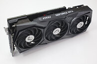
For this, NVIDIA will once again use Samsung's 8 nm DUV node, as it has in the past. The entire NVIDIA "Ampere" architecture lineup was produced on the 8 nm DUV node, and its return after several years was unexpected. We also reported that the rumored RTX 5050 9 GB edition is reportedly on hold, as NVIDIA is pausing the transition from its 8 GB RTX 5050 "Blackwell" version to a 9 GB model due to the reintroduction of the GeForce RTX 3060 12 GB "Ampere" GPU. Since both of these GPUs compete in the budget segment, the company will reportedly only release the older GeForce RTX 3060 12 GB SKU as its primary entry-level design.

Noctua Explains Why chromax.black Fan Releases Take So Long

Austrian fan maker Noctua has published a technical blog explaining why it sometimes takes a long time for the company to release the dark-edition chromax.black fans after the initial beige and brown design is out. The company compares the level of engineering required for a new color code to painting a Formula 1 car, rather than a simple color change like you would typically do with a wooden fence. Noctua is known for its scientific testing, rigorous performance evaluations, highly detailed lab experiments, and more, which make its fans worthwhile. This has created a massive fan base within the enthusiast community over the years, who now eagerly await each new product release. When it comes to manufacturing, the company applies that same rigor everywhere, and a simple color change is not taken lightly. For example, Noctua produces its fans using injection molding, where plastic is melted and forced into a steel mold. However, when a new pigment is used, the entire calculation can be disrupted.

Noctua designs its fans with high precision to maximize airflow performance. This means that blade impellers have a tip clearance before hitting the fan frame of only a few tenths of a millimeter, about 0.5 mm for 120 mm fans and about 0.7 mm for 140 mm fans. Introducing any third-party pigment into this process could disrupt the structure of this fan tip clearance and potentially interfere with Noctua's Sterrox liquid-crystal polymer (LCP) material used in its fans. Specifically, color pigments have particles that directly affect how the injection mold behaves, as they carry their own particle imperfections. This negatively impacts the hundreds of thousands of performance tests that Noctua conducts in the lab and significantly delays the chromax.black product launch.

Apple Reportedly Gives Up on Vision Pro After Disappointing Refresh

According to sources close to MacRumors, Apple is abandoning the development of the next-generation Vision Pro headset after the product failed to capture significant market share. With sales of "only" 600,000 units, Apple has not seen this product line take off as its other products have. Launched in February 2024, the Vision Pro headset debuted with a steep $3,499 price tag. In October 2025, about a year and a half later, Apple updated the Vision Pro with its latest 3 nm M5 SoC, typically used in MacBooks, but even this refresh failed to generate significant interest and orders from users. Although the system offers a technically impressive solution, the market has reacted poorly, particularly due to the high price point Apple set.

Technically, the headset features a micro-OLED 3D display system with 23 million pixels and weighs between 750-800 grams, depending on the headband choice. However, users have complained about the device's weight and distribution, especially around the nose area, which often feels heavy on a single pressure point. No headband choice has been able to completely alleviate this issue. Additionally, the price point is too high for consumers, especially for a technology that is relatively new to the Apple ecosystem. As a result, MacRumors tipsters suggest that Apple is close to completely abandoning the project.

Intel Prepares HBM Killer: HB3DM Memory Stacks with Z-Angle Technology

Intel and SoftBank, through their subsidiary Saimemory, have been developing an alternative technology to the popular high-bandwidth memory (HBM) to provide more bandwidth and capacity for memory modules used with powerful AI accelerators. At VLSI 2026 in June, Saimemory is scheduled to present a paper on the newly developed HB3DM memory, which is based on Z-Angle Memory (ZAM) technology. This name refers to the vertical (Z-axis) stacking of dies, similar to traditional HBM. However, Intel aims to achieve impressive results using state-of-the-art manufacturing technology. The first generation of HB3DM will feature a total of nine layers, stacked using a hybrid bonding technique for 3D chip placement. At the base will be a logic layer that manages data movement within the chip, with eight DRAM layers on top for data storage. Each layer will include about 13,700 TSVs for hybrid bonding.

In terms of capacity, HB3DM will offer about 1.125 GB per layer, translating to 10 GB per memory module. Intel can achieve approximately 0.25 Tb/s of memory bandwidth per mmΒ², and for a 10 GB module with a 171 mmΒ² die area, we can expect around 5.3 TB/s per module. These impressive figures could quickly overshadow competing HBM4 memory, as HB3DM offers much higher bandwidth. HBM4 provides speeds of around 2 TB/s per stack, less than half of what HB3DM will deliver. However, HB3DM is limited by capacity, with only 10 GB available, whereas HBM4 can reach up to 48 GB per stack. Intel may increase the number of layers in production as HB3DM progresses, but for now, it is emerging as a bandwidth leader.

Intel 18A-P Node Delivers 9% Performance Increase and 18% Power Savings

Intel's next-generation 18A node is ready, and the company has tested it, showcasing some impressive results. At the VLSI 2026 Symposium in Honolulu, Hawaii, Intel will present its new research on the capabilities of the upcoming 18A-P node. According to the paper, the 18A-P node can deliver a 9% performance increase at the same power level or achieve 18% power savings at the same performance level compared to the standard 18A. However, there is more to this than meets the eye. Typically, node generations show similar performance and power improvements across generations. What would be expected in terms of power and performance improvements when transitioning from 18A to 14A is now already available with the 18A-P node, but without any density improvements. This makes the 18A-P node a very attractive option for external customers who expect the transistor density of the 18A node found in "Panther Lake," but with significantly better characteristics.

For reference designs, Intel uses an Arm core sub-block to test frequency and power scaling. The new 18A-P node can yield much better results on paper, but one of the most interesting improvements is in manufacturing, specifically in something called skew corners. When a node is manufactured, no two transistors are identical due to the inherent physics of the manufacturing process, especially at today's scale. These variations are measured between fast and slow "corners," meaning faster and slower transistors. The skew refers to how wide the performance and power gap is between these transistors. Intel has managed to improve the skew corners on the 18A-P node by 30% compared to the standard 18A, meaning that power and performance characteristics are now more predictable, especially for parametric yields. This means that chip functions are now more predictable, and Intel has to deal with far fewer variations with the new node.
Below is Intel's paper abstract about the 18A-P node.

Intel Stock Surges to All-Time High on Foundry Revival and Strong CPU Demand

Intel's stock is one of the best-performing semiconductor-related names in 2026, with the company's share price reaching a new all-time high of $94.10 per share at the time of writing. This is remarkable news, considering that about a year ago, Intel's stock hit a decade-low of $17.67 per share. This marks a growth of more than 400% in a single year for a company that is one of the most strategically important in the United States' sovereign semiconductor manufacturing. Intel's rise began with investment from the United States government, aimed at supporting the only company left in the U.S. conducting R&D and advanced silicon manufacturing. Since then, Intel has been on an upward trajectory, and the share price shows no signs of slowing down.

Contributing to this success is the revival of Intel's Foundry business, which is on track to attract many external customers. Intel Foundry recently achieved a significant milestone by improving yields across all major foundry nodes currently in high-volume manufacturing. This includes the Intel 4, Intel 3, and 18A nodes, which power the majority of Intel's product portfolio. In the latest Q1 2026 earnings call, Intel CFO David Zinsner noted that the company continues to improve yields on its older nodes, such as Intel 4 and Intel 3, while refining the yield of the current top-performing 18A node to reduce waste and increase the number of functional chips, even in larger dies. Additionally, Tesla signed on as Intel's first major 14A customer for Elon Musk's Terafab AI chip complex in Austin, indicating that the foundry's success in attracting external clients is just beginning.

Blind Test Shows Gamers Prefer NVIDIA DLSS 4.5 Over AMD FSR 4.1

Back in February, ComputerBase conducted a large blind test comparing in-game screenshots generated using the latest upscaling technologies: AMD's FSR 4.0 and NVIDIA's Deep Learning Super Sampling 4.5. The testing has since been updated, and community votes have been processed, revealing that AMD's updated upscaling technology, FSR 4.1, shows significant improvement over FSR 4.0. However, it still trails behind NVIDIA's DLSS 4.5 in visual quality. In the latest ComputerBase testing, the following games were upscaled using FSR 4.0, FSR 4.1, and DLSS 4.5: Year 117 - Pax Romana, ARC Raiders, Assassin's Creed Shadows, Call of Duty: Black Ops 7, Kingdom Come 2: Deliverance, Resident Evil Requiem, and The Last of Us Part I. In all of these games, the ComputerBase review concluded that DLSS 4.5 was the top performer, a view confirmed by the community in a separate blind test vote.

Similar to the previous test, the ComputerBase team conducted the comparison using videos labeled with three options, without revealing which rendering method was used, to ensure a fully blind test. This resulted in a community verdict with two notable outcomes. First, NVIDIA's DLSS 4.5 remains the leader in image quality, with 6 out of 7 games showing the best results using DLSS 4.5. The only game where AMD's FSR upscaling came out on top was Resident Evil Requiem, where DLSS 4.5 placed second behind FSR 4.1. Overall, DLSS 4.5 is seen as providing sharper visual details and more consistent frame generation compared to AMD's FSR upscaling.

Palit Confirms: GALAX, KFA2, and HOF Branding to Continue

Today, we reported that GALAX is ending its operations as an independent company and integrating into its parent company, Palit. However, users were left wondering whether Palit would stop offering GALAX-branded products, which have significant recognition among gamers. The official company response is that the branding will continue to be active. This means that GALAX-branded Hall-of-Fame (HOF) GPUs for extreme overclocking, the KFA2 brand for Europe, and other GALAX-branded products will remain available on the market. In simple terms, this is just a corporate structure change, with Palit consolidating its ventures under one roof as the parent company. Ongoing customer commitments, including RMA, warranty claims, and general support, will now be handled by Palit, while the design and development of new GPUs under the GALAX brand will continue.
Below is a complete statement from Palit, followed by a statement from GALAX.

GALAX Shuts Down, Famous GPU Vendor Taken Over by Palit After 30 Years

The legendary maker of Hall of Fame (HOF) GeForce GPUs, known for their exceptional overclocking capabilities, GALAX, is officially closing its operations after 30 years in business. GALAX, along with its KFA2 brand for the European market, will now be closed, with existing product inquiries managed by Palitβ€”one of the largest GPU add-in card (AIC) manufacturers and a significant NVIDIA partner. Founded in Hong Kong in 1994, GALAX distinguished itself by creating high-performance designs with NVIDIA GeForce GPUs, particularly known for its HOF series. These iconic white-themed designs feature massive VRM circuitry for overclocking and higher-binned dies suitable for LN2 extreme overclocking scenarios. Over the past few generations, multiple world overclocking GPU records were achieved with GALAX HOF cards, and the brand has maintained that design language throughout the years.

After more than 30 years in business, GALAX is closing its operations, and these will be transferred to Palit, which will take full responsibility for "all activities and commitments related to the brand." This includes RMA services, warranty claims, product launches, and more. Interestingly, the announcement does not mention that the GALAX branding will be phased out. Only the actual company operations will be integrated into Palit. It's possible that Palit will retain the GALAX branding and its HOF name, which is well-known for high-performance overclocking among enthusiasts. It's worth noting that GALAX and its sister brand KFA2 have been operating for years with Palit's support as the parent company, so it's uncertain if the brand will continue its market presence under different management. GALAX and KFA2 have been sub-companies of Palit, and management claims that now is the time to unite all of Palit's brands under one roof.

Update 11:05 UTC: Palit confirmed that the current GALAX branding will continue to be present on the market.

EU Now Requires USB-C Charging for New Laptops Up to 100 W

The European Union has officially imposed a new rule for selling laptops with a power rating of 100 W or less, requiring them to use a USB-C port for charging. This rule takes effect today, April 28, Tuesday, as the European Commission has been exploring ways to reduce electronic waste and has been planning this since imposing a similar rule on smartphones in 2024. As readers may recall, modern smartphones have largely been shipping with USB-C ports since the European Commission mandated that all newly sold smartphones must have a unified connection, instead of multiple connectors that create a significant amount of e-waste across Europe. With laptops, the EU legislation now aims to address this issue in the laptop sector, as they contribute significantly to the problem.

However, there are exceptions to this rule. The traditional USB-C power delivery mechanism can deliver 240 W through a single port, but gaming laptops sometimes require more power. Gaming laptops can continue to use the typical barrel power connector on models that exceed 100 W of power, whereas any laptop model with a power rating of 100 W or less must adopt USB-C as its primary charging connector. From today, it is illegal to sell laptops that do not meet the European Commission's standards across the European Union. However, this rule does not apply to computers sold on the second-hand market; only new devices entering the EU zone must comply.

Microsoft's Shader Model 6.10 Opens Direct Access to GPU AI Engines

Microsoft has released the Shader Model 6.10 preview, included in the new AgilitySDK 1.720-preview build. This preview introduces a compelling feature related to GPU-dedicated AI engine control. According to the developer blog, Shader Model 6.10 features a new, streamlined algebra matrix API that reveals all known matrix operations for popular gaming GPUs from AMD, Intel, and NVIDIA. This means that modern GPUs have dedicated hardware for processing AI workloads, typically involving matrix multiplication and accumulation. Modern machine learning-based upscaling relies on this hardware, whether it's Tensor cores from NVIDIA, XMX cores from Intel, or AI accelerators in AMD GPUs, each with its own communication method. To unify access, Microsoft is introducing a new API from the class linalg::Matrix, which will expose all matrix operations to the shader language. This allows neural rendering operations to be executed across multiple GPUs with a single programming effort.

As the developer behind the DirectX 12 API, Microsoft is observing a significant increase in graphics features utilizing neural network-based rendering techniques to enhance user graphics. This will require more matrix units in modern gaming GPUs. To provide a unified layer of abstraction for programming and executing neural rendering operations, Microsoft hopes that Shader Model 6.10 will become the standard for every GPU maker. Interestingly, this feature is supported across all NVIDIA RTX hardware, as it includes Tensor cores. Intel support is planned for an upcoming release, with B-series GPUs expected to be compatible. Only AMD's RDNA 4-based Radeon RX 9000 series GPUs support this feature, with no support planned for older models like the RX 7000 series and below.

NVIDIA Officially Launches GeForce RTX 5070 Laptop GPU with 12 GB GDDR7 Memory

NVIDIA has officially launched its new GeForce RTX 5070 12 GB laptop edition GPU, featuring higher-capacity GDDR7 memory. This confirms earlier rumors about an upgraded memory configuration. In a quiet release, NVIDIA announced its decision to use 24 Gb (3 GB) GDDR7 memory modules, which offer a 50% increase in memory capacity compared to the current 16 Gb (2 GB) GDDR7 configurations. As demand for GPU memory remains high, NVIDIA can balance the supply of 16 Gb GDDR7 modules by utilizing a new batch of 24 Gb GDDR7 modules from partners like SK hynix, Samsung, and Micron. The company describes this move as a way to ensure a sufficient supply of 16 Gb GDDR7 memory for the remaining GeForce RTX 50-Series "Blackwell" GPUs, maintaining healthy supply levels. The new GPU SKU complements the existing RTX 5070 8 GB Laptop Edition model, providing gamers with more laptop configurations to choose from.
NVIDIADemand for GeForce RTX GPUs remains strong, and memory supply is constrained. In order to maximize memory availability, we are releasing the GeForce RTX 5070 Laptop GPU 12 GB configuration with 24 Gb G7 memory. This gives our partners access to an additional pool of memory to complement the 16 Gb G7 supply that currently ships with most GeForce GPUs. The 12 GB configuration will exist alongside the current 8 GB configuration, and allows our partners to bring a broader range of GeForce RTX 5070 laptops to consumers.

Steam Controller Goes Official on May 4 with $99 Price Tag

Valve has officially confirmed that its highly-anticipated Steam Controller will go on sale globally on May 4. It will be priced at $99 in the United States, €99 in European Union countries, Β£85 in the UK, $149 CAD in Canada, and $149 AUD in Australia, marking a truly global launch. Designed as a universal control device, the Steam Controller aims to be a versatile gamepad for the broader Steam ecosystem, supporting PCs, laptops, Steam Deck, Steam Machine, and even the Steam Frame VR headset. While maintaining familiar core controls, Valve is clearly focusing on additional inputs, including dual trackpads, a gyro, Grip Sense, and four rear grip buttons, all of which can be customized through Steam Input.

Interestingly, Valve has revealed more details about some of the core technology behind the Steam Controller, with perhaps the most intriguing being magnetic thumbsticks built around TMR technology. Valve claims they offer a better feel, improved responsiveness, and much greater durability. They also add capacitive touch support for motion-based controls, meaning your commands can now be expressed in multiple ways. There is also a new puck accessory that handles both wireless connectivity and charging, snapping onto the controller magnetically to serve as a dock and transmitter in one.

Intel Turns Scrap Dies Into Usable CPUs as Demand Keeps Rising

We have been reporting on the intense demand in the CPU sector currently sweeping the industry. AMD and Intel have sold out their inventories, and lead times are now weeks long. However, Intel, which manufactures a large part of its CPU portfolio, has been handling the situation differently. According to Intel and confirmed by industry analyst Ben Bajarin, the company is repurposing some of the dies found on the very edge of the silicon wafer, which would have otherwise become silicon scrap, into products that customers are eager to buy. This approach allows even some SKUs, which may have been flawed due to various effects like silicon node yield, to find new life through repurposing. Intel's customers are so eager for CPUs that higher-end parts, which would typically be discarded, are now being sold as independent SKUs. No silicon is left behind.

For example, when Intel produces a Xeon 6 "Granite Rapids" CPU on the Intel 3 node, the CPU compute die can accommodate up to 44 cores per die, but some are disabled for yield and power reasons. When the yield fails, these compute dies are repurposed into SKUs with lower core counts, as it costs Intel money to manufacture the die, and wasting it would be a significant loss of resources. However, when the die doesn't achieve satisfactory yield on the Intel 3 production line, the company would usually discard it if it can't extract a reasonable number of working cores. Amidst one of the highest-ever recorded CPU shortages, Intel is doing the opposite. The company is using these defective or scrap dies and packaging them into lower-class SKUs to sell to its customers, as any CPU availability is crucial, and customers are eagerly purchasing them. Imagine a wafer edge, which is round, having only a few working P-Cores, and that being packaged into a CPU that a hyperscaler would integrate into their offering.

Intel "Wildcat Lake" Outruns Apple's MacBook Neo and Its Successor in First Benchmarks

Intel recently unveiled its "Wildcat Lake" Core 300 series of laptop processors, designed for the entry-level market with excellent CPU and GPU capabilities to meet basic needs. By combining two "Cougar Cove" P-cores with four LPE "Darkmont" cores, these processors should provide sufficient CPU power for basic tasks in the entry-level segment. Especially when paired with the NPU 5, Xe display and media engine, and a GPU featuring up to two Xe3 cores, this SoC should handle tasks with ease, including some very light entry-level gaming. Today, the first benchmarks appeared, showcasing what this CPU is capable of and how it compares to industry-leading solutions in this price range, such as Apple's newest MacBook Neo, thanks to the initial PassMark benchmark results.

In the latest benchmark, PassMark recorded the Intel Core 5 320 "Wildcat Lake" with two P-cores running at up to 4.6 GHz and LPE cores with a maximum turbo frequency of 3.4 GHz. This SoC scored about 4,047 points in the single-threaded rating and approximately 15,222 in the multithreaded rating in the PassMark evaluation benchmark. This places its rating just above Apple's first-generation M1 SoC in both single and multithreaded results. Additionally, the design surpasses Apple's A18 Pro SoC in the current MacBook Neo and the A19 Pro SoC that is expected to be included in the second-generation MacBook Neo design scheduled for 2027. Technically, both are based on different architectures, but they serve the same purpose: providing customers with an affordable SoC/laptop design that delivers solid computing power for all basic tasks.

Steam Controller to Arrive on May 4 in Japan

Valve's Steam Controller is reportedly just a few days away from launch, as the company is preparing for a May 4 release in Japan. According to a now-deleted post by 4Gamer, the Japanese launch is expected on May 4, with a price of $99. This price includes the controller, a charging cable, and a 2.4 GHz dongle for wireless connectivity to a PC. The removed 4Gamer post mentioned the exact launch time as May 4 at 15:00 local time in Japan, which means the launch timing will differ for the Western hemisphere. This effectively sets the launch date exactly a week from the time of writing, confirming rumors of an imminent release. As a reminder, Valve's Steam Controller will feature elements that justify its $99 price point, including four programmable buttons, dual touchpads, a hall effect sensor, HD rumble for haptic feedback, decent battery life, and connectivity options that include Bluetooth and a separate 2.4 GHz dongle.

Below are some pictures from the 4Gamer article, which has now been taken down.

No New Intel Arc Gaming GPUs? Xe3 Skipped, Xe4 "Druid" Uncertain

Intel's Arc gaming GPU roadmap is in a weird state, as the company has reportedly been reshuffling a significant portion of its dedicated Arc desktop GPU launches for the upcoming quarters. Currently, Intel offers its second-generation "Battlemage" architecture, based on the Xe2 IP, as a dedicated desktop gaming GPU in the form of the B580 mid-range graphics card. For those interested in Xe3-based "Celestial" or Xe3P-based "Crescent Island" dedicated GPU variants, Intel leaker Jaykihn has confirmed that there won't be an update anytime soon. Even the next-generation Xe4 "Druid" is being reconsidered for dedicated gaming GPUs. Intel has previously confirmed that it will continue GPU development, but desktop gamers might not be the primary focus, leaving notebook users in a better position.

Intel currently offers new GPU IP through integrated graphics, such as the Arc B390 iGPU found in "Panther Lake" processors, which use Xe3 IP. However, desktop dedicated GPUs are still using Xe2, and even for a maxed-out "Battlemage" configuration, Intel only offers the Arc Pro B70 and Arc Pro B65 graphics cards. These cards maximize the BMG-G31 Xe2 silicon but are intended for professional users. A recent driver update added the ability to play games on these cards, but they are still primarily designed for AI workloads and professional visualization, and they are priced higher than what the average gamer would want. Gamers are still seeking clarity about future updates, and the lack of recent rumors regarding an additional Arc gaming discrete GPU is concerning. Below are older roadmaps, and we expect to see an updated version sometimes in the near future as Intel confirms changes.

Windows 11 Updates Can Now Be Skipped and Even Paused Indefinitely

Microsoft is... giving users exactly what they want? In the latest Windows Insider preview for Windows 11, Microsoft is rolling out an updated Windows Update experience that gives users more control over their update process. This includes the option to skip updates entirely during the out-of-box experience (OOBE) menu, allowing you to set up a PC without applying updates first. Previously, new PC configurations and installations might have been several months behind on Windows 11 updates, and Microsoft would force users to apply these updates immediately. This led to prolonged OS setup times and user frustration. Now, for those who need to move to a new desktop quickly and apply updates at a later date, Microsoft is finally offering an option during OOBE to install the OS first and apply updates later.

Additionally, Microsoft is now allowing users to pause Windows 11 updates in the settings with a dedicated calendar that extends up to 35 days. This ensures you have ample time to schedule an update session without disrupting your workflow. However, the 35-day mark is not a hard stop, as users can re-pause updates for another 35 days even after the original period has expired, essentially allowing updates to be paused indefinitely. There are no limits on how many times you can reset this pause date, giving you full control over the entire update process. This could be especially useful when a new update series arrives, and you want to wait and see if there are any OS issues or known problems before applying the update. For example, in the latest Windows 11 April update, some PCs might experience a BitLocker trigger, but this will be resolved in a future fix. Users can wait a few days for a fix to arrive and then install updates all at once without being forced to do so immediately.

Apple Set to Become Third-Biggest Laptop Maker This Year

Apple is reportedly set to become the third-largest laptop vendor by the end of 2026, according to market research firm Sigmaintell. Their projections indicate that Apple-made laptops will surpass the industry staple Dell, securing the third spot. This is a remarkable achievement for Apple, which will capture significant unit sales with its newly released, affordable MacBook Neo. According to the market research, the largest vendor by unit sales in 2026 is expected to be Lenovo with 43 million units, followed by HP with 39 million units. Apple is anticipated to sell 28 million MacBooks that year, an impressive number considering the firm sold about 23 million MacBooks in 2025.

The latest MacBook Neo is projected to sell around 10 million units, while the remaining 18 million units are expected to come from the MacBook Air and MacBook Pro 14/16 variants. With its current product portfolio, Apple covers a wide range of market segments, from the entry-level $599 MacBook Neo (or $499 with a student discount) to mid-range offerings like the thin and light MacBook Air, and high-end options for professionals with the MacBook Pro lineup. By catering to every segment from entry-level to high-end, Apple enhances its market visibility and provides users with options to fit their budgets.

Steam Controller to Arrive with $99 Price Tag

Valve's upcoming Steam Controller is one of the most anticipated hardware releases the company plans to unveil soon. In a leaked video review that has since been taken down, we learned that Valve has reportedly priced this product at $99. This price point may leave enthusiasts weighing the potential higher cost against its features. While it is on the pricier side for a wireless controller, Valve positions the Steam Controller as having an ergonomic, programmable, and immersive design. What makes it special are its features, including four programmable buttons, dual touchpads, a hall effect sensor, HD rumble for haptic feedback, decent battery life, and connectivity options that include Bluetooth and a separate 2.4 GHz dongle. All of this may justify the asking price, but given the recent influx of high-quality third-party controllers, we should wait for official reviews before drawing any conclusions.

Just a few days ago, Valve quietly uploaded a Steam Controller unboxing video on its Steam platform. However, the video has not been made available for viewing, as attempting to play it results in a "This video has not been processed for streaming" message. This indicates that the launch of the controller is imminent, but since a review was released early, we are likely just a week or two away from the official unveiling. Below is a screenshot from the leaked video review, which has now been taken down.

AMD Launches EXPO 1.2 for CUDIMM and Low-Latency DDR5 Memory

AMD has officially launched its Extended Profiles for Overclocking (EXPO) version 1.2, which expands support for more memory profiles, CUDIMM, and additional features. With this release, AMD aims to introduce more advanced memory tuning profiles to the "Zen 5" platform and its DDR5 memory types, while full support for EXPO 1.2 features is anticipated with the "Zen 6" processor generation. This means that full CUDIMM support for "Zen 5" tuning is still limited, and only "Zen 6" will offer complete CUDIMM support. EXPO 1.2 works with AMD's AGESA, but since AGESA 1.3.0.1 lacks full CUDIMM DDR5 support, this feature is postponed until the next-generation "Zen 6." Current-generation "Zen 5" CPUs on the AM5 socket may be able to use EXPO 1.2, but they won't fully support the new DDR5 memory with an onboard clock driver, instead relying on traditional memory to perform the task. Notably, popular AMD developer 1usmus mentioned that AMD EXPO 1.2 brings the following changes.
  • Support for module geometry.
  • Added support for MRDIMM (CUDIMM and CSODIMM are already supported). AGESA 1.3.0.1 still lacks full CUDIMM support; AMD is preparing this for Zen 6.
  • New! tREFI, tRRDS, tWR, ULL Enableβ€”Unified Latency Lock and VDDP(V).

Intel Z970 Chipset for "Nova Lake-S" to Cover Much of the B860 Motherboard Segment

Intel's upcoming "Nova Lake" Core Ultra 400 series processors will introduce not only a new CPU platform and socket but also a new motherboard chipset segmentation, unlike anything we have seen from Team Blue. According to a well-known leaker, Jaykihn, the new Z970 chipset platform is set to take over much of the space currently reserved for B860 motherboards. Meanwhile, B960 is expected to be positioned lower in the lineup as a value-focused option, often used by Intel's OEM partners for all-in-one builds or mini-PCs. This makes the Z970 the primary choice for a large share of "Nova Lake" builders, not just enthusiasts. Intel's higher-end Z990 boards are still expected to target the most demanding systems, while Z970 seems to bridge the gap between premium and mainstream desktop segments, incorporating many features that the Zx70 chipsets typically reserved from the Bx60 chipset ranges over the past few years.

The most likely scenario is that the Z970 will offer overclocking and wider I/O selection, while the Z990 will focus on more diverse expansion capabilities. The third entry-level B960 boards are expected to be starter NVL platform designs without overclocking support, intended to get the platform up and running with minimal I/O and SSD expansion. One of the biggest attractions of the Z970 would be CPU overclocking support, a key advantage over the B960, which is anticipated to be the more affordable option but without the same tuning flexibility. While the two chipsets may share similar baseline I/O features, motherboard manufacturers are likely to differentiate them through board design, port count, storage support, and overall feature set.

Intel Foundry Improves Yields Across Intel 4, Intel 3, and 18A Nodes

Intel posted strong Q1 2026 earnings results, indicating improvements across multiple verticals, from Intel Products to Intel Foundry divisions. Both groups experienced operational enhancements, but Intel Foundry achieved a significant milestone: yield improvement across all major foundry nodes currently in high-volume manufacturing. This includes Intel 4, Intel 3, and 18A nodes, which power the majority of Intel's product portfolio. In the latest Q1 2026 earnings call, Intel CFO David Zinsner noted that the company continues to improve yields on its older nodes, such as Intel 4 and Intel 3, while refining the yield of the current top-performing 18A node to reduce waste and increase the number of functional chips, even in larger dies.
David Zinsner, Intel CFOIntel Foundry operating loss in Q1 was $2.4 billion, improved $72 million quarter-over-quarter as better yields across Intel 4, Intel 3, and 18A drove higher gross margins. This was mostly offset by increased operating expenses associated with an intentional step-up in Intel 14A investments to support both internal and external customer evaluations. As a reminder, Intel Foundry carries the bulk of the cost associated with the early ramp of Intel 18A, and we expect Intel Foundry's operating loss to improve through the year as 18A continues to ramp into volume and yields improve further. Within the quarter, Intel Foundry delivered output above our expectations, drove steady improvements in yields, and met key 14A milestones.

Intel's Reference "Wildcat Lake" Laptop Mimics Apple MacBook Neo with Aluminium Body

One of the first Intel "Wildcat Lake" laptops has been revealed, showcasing a design language that closely resembles Apple's highly popular $599 MacBook Neo model. Intel's own reference design model features a standard 6-core "Wildcat Lake" configuration with two Xe3 cores and a 17 TOPS NPU, all housed in an aluminium chassis with a bright color theme, similar to Apple's MacBook Neo. The Intel reference design "Wildcat Lake" laptop operates with a 17 W PL1 mode, which measures the base TDP, and a 35 W PL2 for running the new WCL chip at maximum turbo frequency. There is also a high-performance mode for maximizing core performance with a 22 W PL1 base TDP, as well as a mode for fanless operation. In the PL1 power mode at 11 W, WCL chips can function in fanless environments, making them very versatile.

When Intel launched the "Wildcat Lake" Core 300 series of processors, the company aimed to satisfy value-oriented buyers seeking good CPU performance and basic GPU output in small form-factor commercial and edge AI PCs. The platform's hybrid core configuration, combining two "Cougar Cove" P-cores with four LPE "Darkmont" cores, should provide sufficient CPU power for basic tasks in the entry-level segment. Especially when paired with the NPU 5, Xe display and media engine, and a GPU that includes up to two Xe3 cores, this SoC should handle tasks with ease, along with some very light entry-level gaming.

AMD Stock Hits Record High Above $300 as AI Optimism Fuels Rally

AMD's stock has been experiencing a significant rise over the past few months, with the company's share price reaching a record $303.46 at the time of writing and a market capitalization of nearly half a trillion USD, precisely $494.74 billion. Historically, AMD's stock has struggled to match the levels of NVIDIA and, to some extent, Intel. However, the company has seen a massive turnaround with the expansion of AI data centers. AMD has been performing well in the data center space with its EPYC processors and Instinct MI accelerators, and the stock price has followed this upward trajectory. This is AMD's best stock performance yet, supported by a strong current and upcoming product portfolio that has major investors confident in the company's operations, financials, and execution of plans.

AMD is on track to ship its EPYC "Venice" server CPUs with "Zen 6" architecture, the Instinct MI400 series of accelerators for AI training, inference, and HPC workloads, and Pensando "Vulcano" AI NICs, all housed within a rack-scale system called "Helios." Expected to match and exceed NVIDIA's "Vera Rubin" in some areas, AMD will be competitive in the world's largest industry todayβ€”AI data centers. However, the company is not resting on its laurels and has already prepared a 2027 update of this product portfolio for the next-generation AI rack. This execution has instilled confidence in AMD's investors, driving the stock price significantly higher.

TSMC Says Low-NA EUV Will Carry It Further, Delaying High-NA Adoption

Yesterday, TSMC unveiled its latest A13 node preview at the North America Technology Symposium, highlighting the company's ongoing developments. However, the most significant news isn't about a new node but the technology behind it. TSMC announced it would rely on older ASML Low-NA EUV tools instead of the more expensive High-NA EUV scanners. With the High-NA EUV scanner priced at about €350 million ($410 million), the capital expenditure required to equip a modern facility is substantial. TSMC claims it can maintain a competitive advantage using the existing Low-NA EUV technology, which costs roughly half as much per machine. Kevin Zhang, TSMC's deputy Co-COO and SVP, noted to Reuters, "This is where I think our R&D has done exceptionally well in terms of leveraging existing EUV technology while setting an aggressive technology scaling roadmap. This is definitely a strength."

TSMC's use of Low-NA EUV lithography involves a technique called multi-patterning, where the EUV machine takes multiple passes to etch a design on a single layer. By performing two Low-NA etching runs, TSMC can achieve benefits similar to High-NA exposure, effectively reducing the need for new tools. However, there are limitations to the Low-NA multi-patterning technique, which will be addressed later by introducing High-NA systems, but only for nodes at 1 nm and below. For now, and for recent nodes, TSMC sees a way to maximize performance from the existing Low-NA systems at a much lower capital expenditure than would be required for High-NA systems.
❌