Intel Foundry has released a video of a multi-chiplet 2.5D/3D processor with a 10,296 mm^2 silicon footprint, including leading-edge technologies such as 14A and 18A.
A reported attempt by a covert Chinese lab to reverse-engineer an EUV lithography scanner underscores that, despite access to scattered components, replicating ASML's EUV tools is effectively impossible without recreating the company's entire global supply chain, optics ecosystem, and proprietary software built over decades.
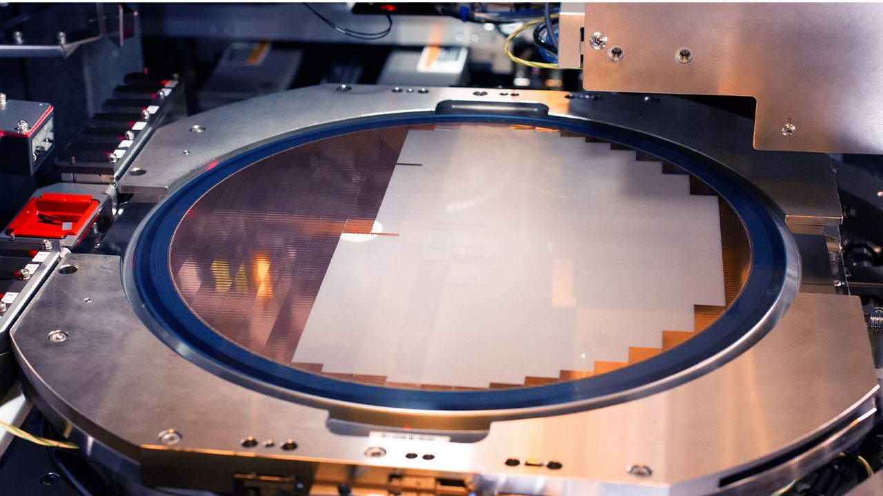
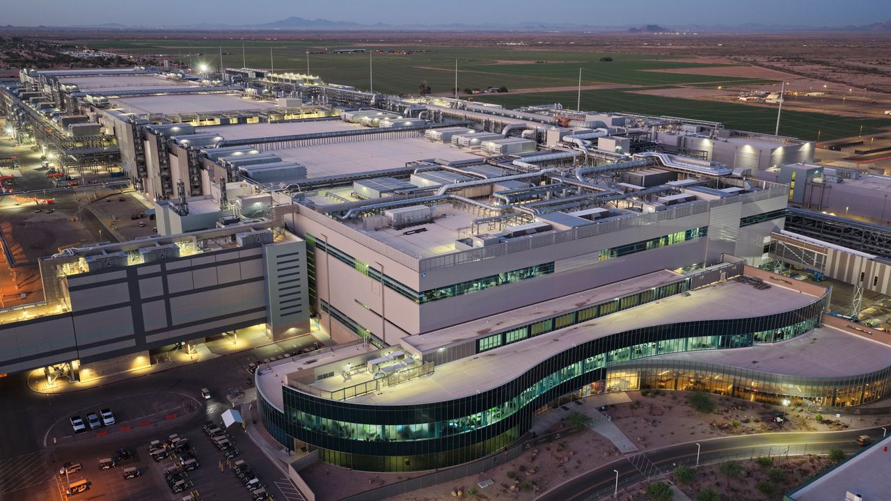
Intel's Fab 52 in Arizona is currently the most advanced chip production facility in America, but it has yet to reach its full 40,000-wafer capacity due to low 18A yields.