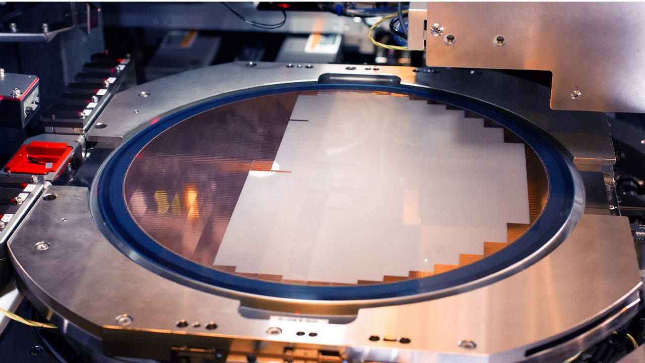
Intel Foundry has released a video of a multi-chiplet 2.5D/3D processor with a 10,296 mm^2 silicon footprint, including leading-edge technologies such as 14A and 18A.
The adjustment comes as China’s largest foundry runs near full utilization and faces sustained demand from domestic customers building inventories of memory and logic chips.
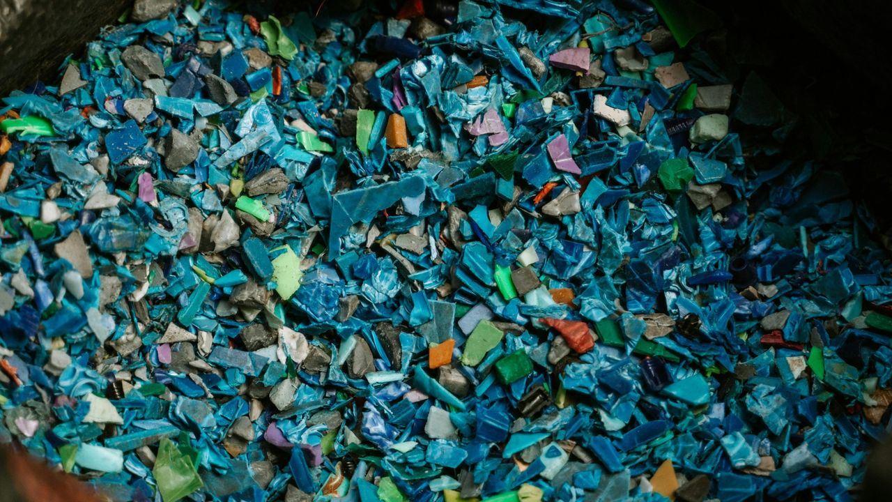
Researchers from Northeastern University discovered that PEDOT:PSS, which is typically used in medical research, breaks down into harmful microplastics.
A reported attempt by a covert Chinese lab to reverse-engineer an EUV lithography scanner underscores that, despite access to scattered components, replicating ASML's EUV tools is effectively impossible without recreating the company's entire global supply chain, optics ecosystem, and proprietary software built over decades.
Nvidia is preparing to deliver up to 80,000 H200 AI chips to China before the Lunar New Year holiday, marking the first time this level of silicon would be legally exported to the country since 2022.
10 former Samsung employees are accused of leaking Samsung's 10-nm DRAM technology to CXMT, allegedly allowing the latter to achieve technological breakthroughs on stolen information.
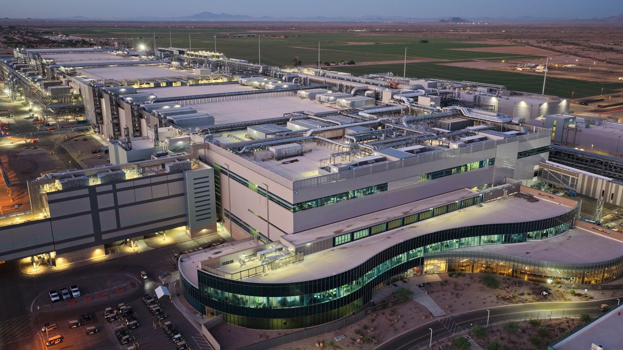
Intel's Fab 52 in Arizona is currently the most advanced chip production facility in America, but it has yet to reach its full 40,000-wafer capacity due to low 18A yields.
Chinese fabs are quietly extending the useful life and performance of older ASML deep ultraviolet lithography systems by upgrading key subsystems, as Beijing pushes to sustain advanced chip output.