❌

Reading view

SK Hynix says 2027 will be the 'worst year' for memory shortage, forecasts crunch to last until 2030 β€” CEO shares grim outlook on the day SK Hynix gets listed on Nasdaq

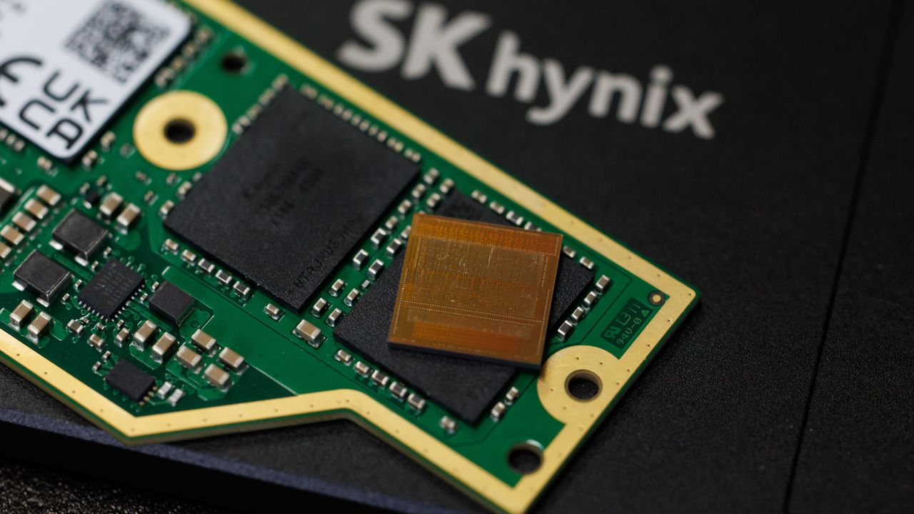
SK Hynix CEO Kwak Noh-jung says that 2027 will be the "worst year" for the ongoing memory shortage in comments shared with Reuters. The remark comes on the heels of SK Hynix successfully marking the largest-ever IPO for a foreign company on the U.S. stock market, raising $26.5 billion. Although Kwak points to next year being the worst for RAM shortages, the executive expects the memory crunch to last until 2030.

"We forecast that next year will be the worst year in the industry's history from the supply perspective," Kwan told Reuters. "We still forecast that customer demand will remain higher than our ​supply capacity even beyond 2030. But we are doing our best to solve the problem."

In March, SK Group chairman Chey Tae-won also suggested shortages would last until 2030, and the company has previously pointed to 2027 as a key shortage point, alongside Samsung. DRAM demand is largely driven by the HBM used in AI accelerators, which require far more sophisticated manufacturing and packaging processes compared to consumer DDR5. On top of advanced manufacturing, HBM also consumes more wafer capacity than DDR5, forcing major memory brands to reallocate supply and double down on an already sticky supply situation.

Forecasts like this are tricky. It's in SK Hynix's financial interest for memory shortages to continue, even well beyond 2030. SK Hynix has set a record for quarter-over-quarter revenue, and rival Micron has seen its stock value increase 213% this year, pushing its share price to around $990.

However, Kwan's remarks aren't just a bid to rally behind SK Hynix stock. Over the past few months, we've seen Micron and SK Hynix ink long-term supply agreements (LTAs). These agreements commit supply over multiple years to particular companies and define a price floor and ceiling during the agreement term. Although LTAs don't directly influence market prices, they secure demand, and we've seen a lot of LTAs over the past several months to bind DRAM supply.

Although memory (and NAND) prices will remain elevated for at least the next several months, we've seen some signs of the market cooling. Earlier this month, a TrendForce report showed DRAM contract prices up 15% to 18% quarter over quarter for Q3 2026. That's a large increase, but far lower than the QoQ increases we've seen previously.

We're nearing some semblance of stability in the memory market, just stability at vastly elevated prices. How long that lasts is anyone's guess. Although memory brands like SK Hynix have visibility into market trends, those can rapidly change. Just this year, we've seen a massive pivot toward AI spending going toward CPUs, pushing Intel's stock to record highs while shedding around $1 trillion in Nvidia's market cap; a year ago, that would've been almost impossible to predict.

AMD EXPO ULL shows middling performance gains in initial tests despite eye-watering price increase β€” first benchmarks show up to a 4% improvement with DDR5-6000 CL36

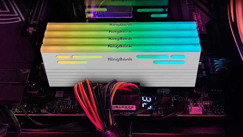
After announcing it last month, the first AMD EXPO Ultra Low Latency (ULL) memory kits are finally available; and with up to an 80% jump over already inflated RAM prices in tow. HardwareLuxx was able to snag a kit of G.Skill's new Trident Z5 NeoX RGB memory to see how ULL performs, and the results don't quite justify the extra cost. At most, the publication found just a 4% improvement compared to non-ULL kits.

That aligns with AMD's original claims about ULL. When the company announced the initiative last month, it also cited a 4% improvement over standard EXPO. However, AMD claims that ULL offers a 4% improvement on average, while HardwareLuxx only found that large of an improvement in a single game: F1 25.

HardwareLuxx tested a 2 x 16GB kit at 6,000 MT/s with primary timings at 36-36-36-76. Compared to standard EXPO/XMP DIMMs, a lot of the optimization with ULL DIMMs comes from tuning the subtimings. The primary timings are largely the same as what you'll find on a standard EXPO kit, short of tWR (write recovery), which is lower on the EXPO ULL kit. Better binning of the memory ICs allows for more aggressive subtiming optimization, as HardwareLuxx notes, rather than relying on timings primarily concerned with stability.

In games, the ULL kit showed clear performance improvements, no matter how minor they were. In F1 25, the ULL kit outclassed a DDR5-6000 CL26-36-36-96 kit by 4.2%, and beat out JEDEC standards at 5600 MT/s by nearly 14%. Similarly, in Cyberpunk 2077, the ULL kit was around 3.7% faster than the standard EXPO kit, and 12.7% faster than JEDEC standards. The outlet also tested Arc Raiders, Baldur's Gate 3, and Counter-Strike 2; however, the ULL kit didn't offer a meaningful performance improvement in any of these titles.

The outlet also tested 7-Zip, though with only minor differences between ULL and non-ULL memory. The most interesting results are from the microbenchmarks available in AIDA64, which HardwareLuxx also ran. ULL showed largely similar copy and read throughput, but write throughput was 9.4% higher with ULL compared to stock EXPO.

Although there's a performance benefit, it's minor, and HardwareLuxx notes that "manual tuning still allows for the maximum possible optimization."

The particular kit that HardwareLuxx tested doesn't have the extreme ULL price increases we've seen elsewhere. It's currently available for sale for $530, which is only $20 more than a kit of G.Skill's Trident Z5 Neo RGB memory at DDR5-6000 CL36. It's actually gone down in price (it was originally listed at $550), while kits with more aggressive timings have increased in price.

The NeoX DDR5-6000 CL26 kit, for example, has jumped up $50 to $1,150 β€” yes, that's for a 2 x 16 GB kit still β€” while the CL28 kit has jumped up to $1,030 (a $30 price increase). Two weeks ago, we saw non-ULL kits selling at $560 and $700 for CL28 and CL26, respectively, creating a large delta in price between ULL and non-ULL kits. Now, those kits are selling for $700 and $900, respectively.

The introduction of ULL couldn't have come at a worse time, as the ongoing DRAM shortage continues to raise the cost of building a PC around the world. Adding a premium on top of those already inflated prices is tough to justify, even if that premium is modest β€” especially for mainstream CL36 and CL30 kits, the "ULL tax" is essentially null. The good news is that you can largely achieve what ULL offers on your own, at least given that you have the patience to sit through tuning your memory for single-digit gains.

JEDEC releases new SPHBM4 standard to slash AI memory costs β€” Narrow 512-bit interface enables dropping expensive interposers for organic substrates

JEDEC has released its new specification that aims to push down the pricing of the ultra-expensive HBM that powers the fastest AI processors. While the new standard will not help relieve the DRAM shortage as it uses large HBM4 DRAM devices, it can make high-bandwidth memory a bit cheaper as it enables attaching SPHBM4 memory stacks without advanced packaging and using inexpensive organic substrates.

The standard's body published the specification of SPHBM4, Standard Package High Bandwidth Memory (JESD330-4), that combines HBM4 DRAM ICs with standard packaging and a fast 'narrow' 512-bit interface. Here are the details.

HBM4 performance with a 512-bit wide interface

Although 1024-bit and 2048-bit interfaces used by HBM3 and HBM4 memory deliver unbeatable performance, their wide interfaces consume significant silicon area inside processors, they require expensive interposers, and advanced packaging technologies with limited capacity, such as TSMC’s CoWoS, for integration with host processors. The upcoming SPHBM4 memory continues to use the same HBM4 DRAM stacks as JESD270-4, but swaps the conventional HBM base die for a new SPHBM4 PHY/buffer die featuring a narrower 512-bit interface that enables mounting on standard organic substrates without using sophisticated packaging methods for integration. To offset the effect of the narrower interface, SPHBM4 supports considerably higher data transfer rates ranging from 22.4 GT/s to 46.0 GT/s.

Instead of connecting to the host processor using a 2048-bit memory interface like HBM4, SPHBM4 uses 32 independent 16-bit DDR channels organized into eight Quad Channels. Since 'Quad Channel' is a new term, let us explain how things work. Internally, an HBM4 stack contains 32 memory channels, each 64 bits wide, for a total external interface width of 2048 bits. SPHBM4 needs to 'convert' the 2048-bit internal I/O onto a 512-bit external interface, which is why it groups every four HBM4 channels into a Quad Channel. As a result, externally, a Quad Channel exposes 64 data pins (4 Γ— 16 bits), which replace the 256 data pins (4 Γ— 64 bits) that those four HBM4 channels would normally require. To preserve bandwidth, these 64 pins operate at four times the data rate of the original HBM4 interface.

While SPHBM4 dramatically increases I/O bandwidth, it does not make the DRAM array itself faster. The HBM4 memory core retains the same fundamental architecture and timings, including core frequency, row activation, precharge, and refresh operations, though the additional PHY is expected to introduce some latency. For example, the DRAM core runs at only one-quarter of the external interface frequency, which means 2 GHz in the case of SPHBM4 with a 32 GT/s speed bin.

The major change is the new base die, which implements a high-speed SerDes-like PHY that maps each 16-bit external channel to four conventional 64-bit HBM4 channels. As a result, SPHBM4 introduces equalization, lane training, BER requirements, and other high-speed signaling features that are unnecessary in HBM4’s slower, wide parallel interface. To support transfer rates of up to 46.0 GT/s/s per pin, each Quad Channel uses a shared command/address interface protected by forward error correction (FEC), while data transfers rely on dedicated differential write (WCK) and read (RCK) clocks, as well as ECC and error-reporting signals.

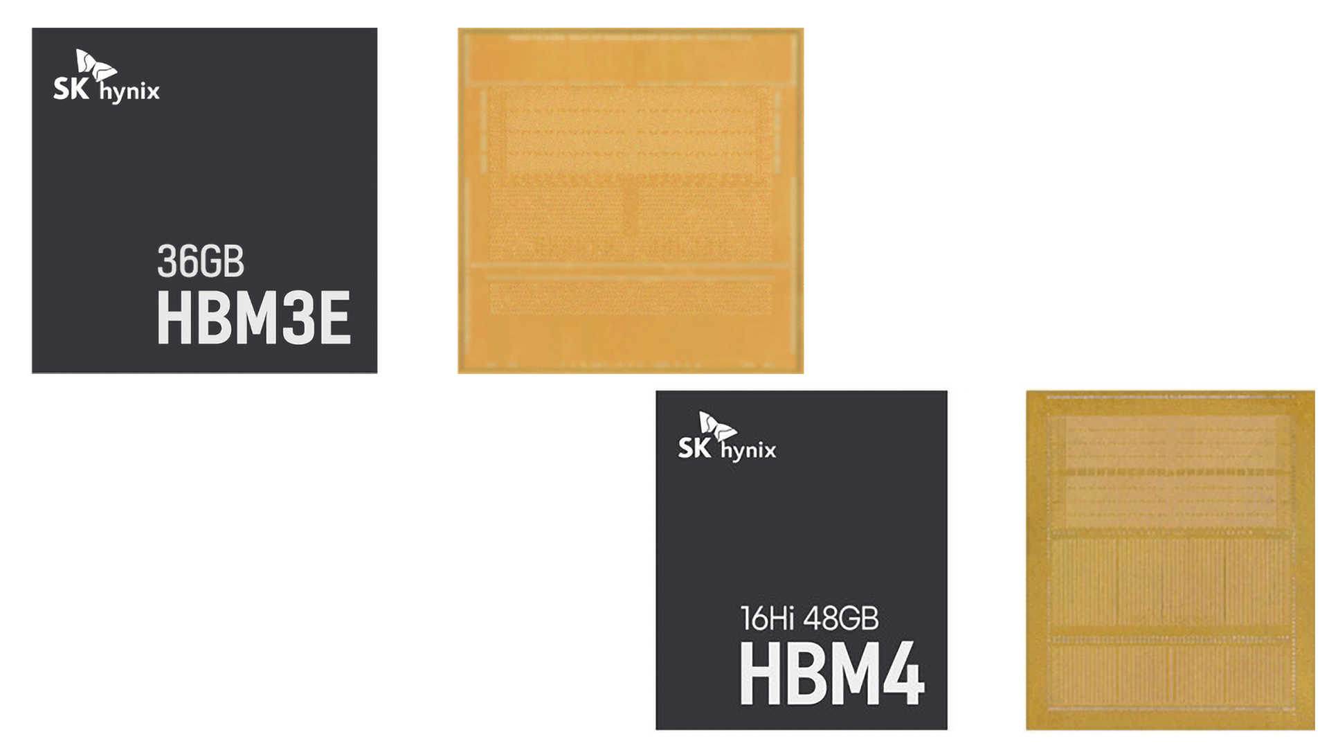
When it comes to capacity, SPHBM4 can use stacks containing 4, 8, 12, or 16 DRAM dies featuring 24 Gb or 32 Gb densities, so the largest standardized SPHBM4 configuration is a 64 GB memory stack built from sixteen 32 Gb DRAM dies, identical to the maximum capacity supported by HBM4E.

Cheap HBM at last?

The standard supports bump pitches greater than 90 Β΅m and channel reaches up to 20 mm, which are two features that enable dropping the expensive interposer and using less-expensive organic substrate routing. However, getting rid of the interposer and CoWoS (or similar) packaging does not automatically make SPHBM4 inexpensive. SPHBM4 still requires massive HBM4 DRAM ICs, 2.5D packaging, a complex base die (which is likely costlier than the one used by conventional HBM4), and advanced package assembly with through-silicon vias. In addition, SPHBM4's narrow interface consumes significantly less die perimeter and silicon area inside processors, which makes it more attractive to companies that strive to install more compute capability and/or intend to install more memory stacks around their processors. However, we are still talking about a niche high-performance memory technology that will address select applications and will barely rival HBM4 directly.

When it comes to maximum performance, HBM4 moves the data at 8 GT/s (though most controllers and chips support higher data rates), so one HBM4 stack can offer bandwidth of 2 TB/s. HBM4E is set to up data transfer rate to 12 – 12.8 GT/s, therefore increasing peak bandwidth to 3 – 3.3 TB/s per stack. By contrast, one SPHBM4 with a 46 GT/s interface can hit 2.944 TB/s, though do not expect the initial versions of SPHBM4 to hit the maximum speed. Therefore, it is likely that HBM4, HBM4E, and C-HBM4E will maintain a performance lead in terms of bandwidth over SPHBM4 in the foreseeable future.

HBM4 latency will still probably have an edge over SPHBM4. HBM4 essentially connects to its host processor almost directly through a very simple interface. By contrast, SPHBM4 inserts a much more sophisticated PHY that performs serialization/deserialization, lane training, FEC handling, and other operations that can add a few nanoseconds of latency. This may not be a big problem for some applications, but inference benefits a lot from low latencies.

When it comes to power and voltages, HBM4 and SPHBM4 share the same DRAM core voltage because SPHBM4 reuses standard HBM4 DRAM stacks. However, I/O is different: HBM4 leaves the interface voltage up to memory vendors and allows implementations at 0.7V, 0.75V, 0.8V, or 0.9V, depending on the desired balance between power, speed, and signal integrity. By contrast, SPHBM4 standardizes the external I/O at 0.75V.

Also, HBM4 moves data over a very wide interface with many slow parallel links that tend to be very energy efficient. By contrast, SPHBM4 moves the same amount of data through one-quarter as many wires, which run roughly four times faster. High-speed data transfer tends to be less energy efficient than 'slow' data transfers over a wide interface. Keeping in mind SPHBM4's rather sophisticated PHY that converts a wide interface into a narrow interface, which is likely a power-hungry process. Nonetheless, the 4X lower number of drivers and receivers could tangibly reduce the power consumption of SPHBM4. That said, without implementation details from DRAM makers or a processor developer, it is impossible to conclude which memory type has lower power consumption.


Last but not least, SPHBM4 essentially trades manufacturing challenges that arise from using silicon interposers for an engineering challenge of developing an extremely sophisticated base die/PHY. Developing and manufacturing such a base die should not be a problem for foundries. However, it remains to be seen whether DRAM makers can design and produce SPHBM4 with decent power efficiency. After all, both Micron and SK hynix work with TSMC to build C-HBM4E and HBM4E base dies, whereas Samsung's memory division uses base dies produced by Samsung Foundry.

China factor

One interesting aspect of SPHBM4 is whether Chinese developers of AI accelerators can benefit from this technology. In theory, Chinese developers like Biren, Huawei, Moore Threads, and other blacklisted companies that cannot use TSMC's chip manufacturing or packaging services could become one of the biggest beneficiaries of SPHBM4, perhaps even more so than the U.S.

First up, a smaller shoreline directly benefits chips that are made using trailing nodes, as it enables packing more compute capability into them without sacrificing memory bandwidth or capacity. Secondly, Chinese OSATs currently do not offer CoWoS-like technologies, so eliminating the interposer and using advanced organic substrates is a benefit.

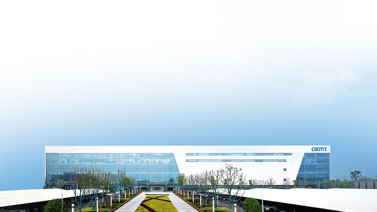
However, SPHBM4 still requires HBM4 DRAM stacks, and today, Samsung, SK hynix, and Micron are the only companies capable of producing them, while China-based CXMT can barely make HBM2E. Furthermore, building a 46 GT/s PHY is very hard and will likely be challenging for Chinese IC developers.

Nonetheless, assembling SPHBM4 packages on organic substrates is arguably more aligned with China's existing manufacturing base, so if local DRAM makers eventually develop competitive HBM4-class memory, SPHBM4 could substantially reduce one of the country's remaining infrastructure gaps.

Summary

JEDEC's SPHBM4 looks like a promising standard that can potentially address a broader range of applications than HBM4 itself due to lower integration cost. Still, HBM4, HBM4E, and C-HBM4E will maintain performance leadership, which will make them a preferable choice for flagship AI accelerators in the coming years.

❌